
Origin of the wide band gap from 0.6 to 2.3 eV in photovoltaic material InN: quantum confinement from surface nanostructure
Abstract
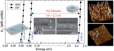
The fierce controversy of the band gap of InN from 0.6 to 2.3 eV has been debated for nearly fifteen years. Numerous possible reasons, such as the Moss–Burstein effect, oxygen incorporation and indium : nitrogen stoichiometry, have been postulated to interpret this outstanding issue. Nevertheless, none of them can provide a convincing and comprehensive explanation. Here, we shed new light on this notable debate using state-of-the-art first-principles calculations based on many-body perturbation theory combined with experiments. We demonstrate that the ubiquitous surface nanostructures (NSs) with amazing characteristics, that is, the outgrowth needle- or dot-like nanocrystals of the InN film surface, are vital and significantly alter its electronic structure and optical properties. The valence band inversion in the decreasing order of crystal-field split-off hole and heavy/light hole can occur in these NSs, which leads to an optical transition switch from E ⊥ c in bulk InN to E ‖ c in surface InN NSs. Moreover, the strong surface bound excitons can be induced in InN NSs due to quantum confinement, resulting in the exciton absorption/emission from infrared to visible (green) wavelength. The blue shift of the PL peak in InN quantum dots with decreasing size further provides convincing evidence for the essence of the large variable band gap of InN. The electronic structure, optical polarization properties and especially the strong exciton effect of InN NSs have been investigated systematically and comprehensively and lays the foundation for future applications of InN QD based photovoltaic and light-harvesting devices.
- This article is part of the themed collection: 2016 Journal of Materials Chemistry A HOT Papers
 Please wait while we load your content...

