
Electronic transport properties of PbSi Schottky-clamped transistors with a surrounding metal–insulator gate

Abstract
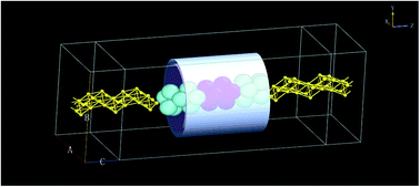
Sustaining Moore's law requires the design of new materials and the construction of FET. Herein, we investigated theoretically the electronic transport properties of PbSi nanowire Schottky-clamped transistors with a surrounding metal–insulator gate by employing MD simulations and the NEGF method within the extended Hückel frame. The conductance of PbSi nanowire transistors shows ballistic and symmetrical features because of the Schottky contact and the resonance transmission peak, which is gate-controlled. Interestingly, the PbSi(8,17) nanowire FET shows a high ON/OFF ratio and proves to be a typical Schottky contact between atoms as described by the EDD and EDP metrics.
 Please wait while we load your content...

