A technique for a nano-textured gapless microlens array using self-formation characteristics of anodic alumina†
 *a
*a
Abstract
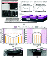
This paper presents a method to utilize the growth properties of anodic alumina possessing self-formation characteristics to fabricate a nano-textured microstructure and also introduces an application technique of the proposed method. The growth rate of anodic alumina, fabricated on aluminum surfaces, has a strong dependence on the intensity of the applied current density or electric field. The uniformity of the thickness of anodic alumina is determined by its electrical distribution characteristics. Accordingly, microscale structures can be fabricated using the growth rate deviation of anodic alumina. A patterned insulative layer is an important factor that determines the current density distribution property of a local region. A computational analysis and a verification experiment can verify this characteristic through the correlation between structural dimensional conditions and a cross-section of the fabricated anodic alumina. The anodic alumina fabricated by the verification experiment in this study had a swollen shape and a nano & micro complex structure, in which a nanoscale base pattern was formed on all bottom surface due to the process characteristics. Based on the advantages of the proposed process, evidenced by the reliability evaluation results, gapless microlens array (MLA) replication molds with nanostructured surfaces were fabricated to verify the applicability of the proposed technique to other fields. A patterned insulative layer with a cylindrical cavity and dimensional conditions was designed to induce the fabrication of lens-shaped anodic alumina. The anodic alumina fabricated by the long process was selectively etched out, and an additional process was conducted to fabricate a nanoporous structure having controlled dimensional conditions on the engraved gapless MLA surface. The textured aluminum surface was used as a replication mold for the imprinting process. The analysis of the fabrication results showed that the gapless MLA surface had a nanopillar structure. In addition, we investigated the reflection characteristics of the fabricated gapless N-MLA structure according to the incident light and verified the low reflectance of the gapless microlens. The results of this study affirmed that the proposed technique is applicable to various fields including those concerning optical devices.
 Please wait while we load your content...

