Covalent bonding-assisted nanotransfer lithography for the fabrication of plasmonic nano-optical elements†

Abstract
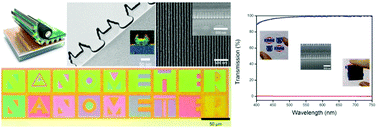
Many high-resolution patterning techniques have been developed to realize nano- and microscale applications of electric devices, sensors, and transistors. However, conventional patterning methods based on photo or e-beam lithography are not employed to fabricate optical elements of high aspect ratio and a sub-100 nm scale due to the limit of resolution, high costs and low throughput. In this study, covalent bonding-assisted nanotransfer lithography (CBNL) was proposed to fabricate various structures of high resolution and high aspect ratio at low cost by a robust and fast chemical reaction. The proposed process is based on the formation of covalent bonds between silicon of adhesive layers on a substrate and oxygen of the deposited material on the polymer stamp. The covalent bond is strong enough to detach multiple layers from the stamp for a large area without defects. The obtained nanostructures can be used for direct application or as a hard mask for etching. Two nano-optical applications were demonstrated in this study, i.e., a meta-surface and a wire-grid polarizer. A perfect absorption meta-surface was generated by transferring subwavelength hole arrays onto a substrate without any post-processing procedures. In addition, a wire-grid polarizer with high aspect ratio (1 : 3) and 50 nm line width was prepared by the nano-transfer of materials, which were used as a hard mask for etching. Therefore, CBNL provides a means of achieving large-area nano-optical elements with a simple roll-to-plate process at low cost.
 Please wait while we load your content...

