
Roles of conducting filament and non-filament regions in the Ta2O5 and HfO2 resistive switching memory for switching reliability

Abstract
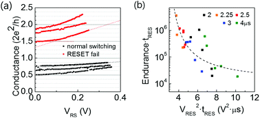
The endurance of switching cycles, which is a critical measure of device reliability, in an ultra-thin (1.5 nm) Ta2O5 and HfO2 resistive random access (ReRAM) memory cell with a 28 nm lateral dimension was studied using current–voltage (I–V) sweep and closed-loop pulse switching (CLPS) tests. The two devices showed the typical oxygen-deficient conducting-filament (CF)-mediated bipolar resistance switching behaviour, which was induced by the asymmetric electrode configuration: Ta as the oxygen vacancy (VO) source/reservoir and TiN as the inert electrode. In these device geometries, the CF is supposed to initiate at the oxide/TiN interface and to grow towards the Ta electrode during the switch-on process, while the switch-off process was induced by the contraction of the CF from the Ta/oxide interface. Both devices, however, showed inversion (anomalous SET; switching from the off- to on-state) behaviour in the RESET (switching from the on- to off-state) process, which can be explained by the authors’ previous model of the hourglass-shaped CF. In this model, once the CF is ruptured, the RESET polarity bias makes the lower portion of the CF regrow to slightly reconnect such a CF through the accelerated migration of VO from the upper-portion CF to the lower-portion CF, which induces switching performance degradation. In the I–V sweeps, the on- and off-states of the devices showed an overall conductance difference approximately corresponding to the integer multiple values of quantum point contact (G0), but there were arbitrary 0.25 and 0.125G0 differences in the conductance values of the on-state for the Ta2O5 and HfO2 devices, respectively. This suggests that these are the minimal units of conductance variation even for a given CF with a standard G0. Although the precise reason for the emergence of such an abnormal conductance unit is not yet understood, its implication for the reliability is critical. Reliable resistive switching was achieved only for the cases where the minimum point conductance was retained even in the off-state; in the other cases, over-SET and over-RESET were induced, which eventually degraded the device reliability. The detailed quantitative analysis of the device failure revealed that the increasing concentration of VO within the non-CF region in the cell decreased the resistance values of that region, which eventually resulted in the over-SET and over-RESET behaviours during the CLPS tests.
 Please wait while we load your content...

