Photoresponse of atomically thin MoS2 layers and their planar heterojunctions†
Abstract
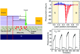
MoS2 monolayers exhibit excellent light absorption and large thermoelectric power, which are, however, accompanied by a very strong exciton binding energy – resulting in complex photoresponse characteristics. We study the electrical response to scanning photo-excitation on MoS2 monolayer (1L) and bilayer (2L) devices, and also on monolayer/bilayer (1L/2L) planar heterojunction and monolayer/few-layer/multi-layer (1L/FL/ML) planar double heterojunction devices to unveil the intrinsic mechanisms responsible for photocurrent generation in these materials and junctions. A strong photoresponse modulation is obtained by scanning the position of the laser spot, as a consequence of controlling the relative dominance of a number of layer dependent properties, including (i) the photoelectric effect (PE), (ii) the photothermoelectric effect (PTE), (iii) the excitonic effect, (iv) hot photo-electron injection from metal, and (v) carrier recombination. The monolayer and bilayer devices show a peak photoresponse when the laser is focused at the source junction, while the peak position shifts to the monolayer/few-layer junction in the heterostructure devices. The photoresponse is found to be dependent on the incoming light polarization when the source junction is illuminated, although the polarization sensitivity drastically reduces at the monolayer/few-layer heterojunction. Finally, we investigate the laser position dependent transient response of the photocurrent to reveal that trapping of carriers in SiO2 at the source junction is a critical factor to determine the transient response in 2D photodetectors, and also show that, by a systematic device design, such trapping can be avoided in the heterojunction devices, resulting in a fast transient response. The insights obtained will play an important role in designing a fast 2D TMD based photodetector and related optoelectronic and thermoelectric devices.
 Please wait while we load your content...

