The effects of shell layer morphology and processing on the electrical and photovoltaic properties of silicon nanowire radial p+–n+ junctions
Abstract
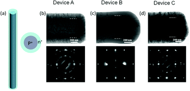
Single wire p+–n+ radial junction nanowire solar cell devices were fabricated by low pressure chemical vapor deposition of n+ silicon shell layers on p+ silicon nanowires synthesized by vapor–liquid–solid growth. The n+-shell layers were deposited at two growth temperatures (650 °C and 950 °C) to study the impact of shell crystallinity on the device properties. The n-type Si shell layers deposited at 650 °C were polycrystalline and resulted in diodes that were not rectifying. A pre-coating anneal at 950 °C in H2 improved the structural quality of the shell layers and yielded diodes with a dark saturation current density of 3 × 10⁻⁵ A cm−2. Deposition of the n-type Si shell layer at 950 °C resulted in epitaxial growth on the nanowire core, which lowered the dark saturation current density to 3 × 10⁻⁷ A cm−2 and increased the solar energy conversion efficiency. Temperature-dependent current–voltage measurements demonstrated that the 950 °C coated devices were abrupt junction p+–n+ diodes with band-to-band tunneling at high reverse-bias voltage, while multi-step tunneling degraded the performance of devices fabricated with a 950 °C anneal and 650 °C coating. The higher trap density of the 950 °C annealed 650 °C coated devices is believed to arise from the polycrystalline nature of the shell layer coating, which results in an increased density of dangling bonds at the p+–n+ junction interface.
 Please wait while we load your content...

