
Current transport mechanism at metal–semiconductor nanoscale interfaces based on ultrahigh density arrays of p-type NiO nano-pillars†
Abstract
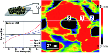
The present work focuses on a qualitative analysis of localised I–V characteristics based on the nanostructure morphology of highly dense arrays of p-type NiO nano-pillars (NiO-NPs). Vertically aligned NiO-NPs have been grown on different substrates by using a glancing angle deposition (GLAD) technique. The preferred orientation of as grown NiO-NPs was controlled by the deposition pressure. The NiO-NPs displayed a polar surface with a microscopic dipole moment along the (111) plane (Tasker's type III). Consequently, the crystal plane dependent surface electron accumulation layer and the lattice disorder at the grain boundary interface showed a non-uniform current distribution throughout the sample surface, demonstrated by a conducting AFM technique (c-AFM). The variation in I–V for different points in a single current distribution grain (CD-grain) has been attributed to the variation of Schottky barrier height (SBH) at the metal–semiconductor (M–S) interface. Furthermore, we observed that the strain produced during the NiO-NPs growth can modulate the SBH. Inbound strain acts as an external field to influence the local electric field at the M–S interface causing a variation in SBH with the NPs orientation. This paper shows that vertical arrays of NiO-NPs are potential candidates for nanoscale devices because they have a great impact on the local current transport mechanism due to its nanostructure morphology.
 Please wait while we load your content...

