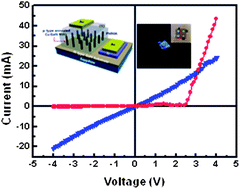
GaN has been utilized in optoelectronics for two decades. However, p-type doping still remains crucial for realization of high performance GaN optoelectronics. Though Mg has been used as a p-dopant, its efficiency is low due to the formation of Mg–H complexes and/or structural defects in the course of doping. As a potential alternative p-type dopant, Cu has been recognized as an acceptor impurity for GaN. Herein, we report the fabrication of Cu-doped GaN nanowires (Cu:GaN NWs) and their p-type characteristics. The NWs were grown vertically via a vapor–liquid–solid (VLS) mechanism using a Au/Ni catalyst. Electrical characterization using a nanowire-field effect transistor (NW-FET) showed that the NWs exhibited n-type characteristics. However, with further annealing, the NWs showed p-type characteristics. A homo-junction structure (consisting of annealed Cu:GaN NW/n-type GaN thin film) exhibited p–n junction characteristics. A hybrid organic light emitting diode (OLED) employing the annealed Cu:GaN NWs as a hole injection layer (HIL) also demonstrated current injected luminescence. These results suggest that Cu can be used as a p-type dopant for GaN NWs.
You have access to this article
 Please wait while we load your content...
Something went wrong. Try again?
Please wait while we load your content...
Something went wrong. Try again?


