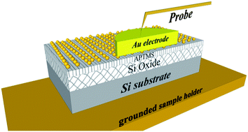
Electrical transport studies across nm-thick dielectric films can be complicated, and datasets compromised, by local electrical breakdown enhanced by nm-sized features. To avoid this problem we need to know the minimal voltage that causes the enhanced electrical breakdown, a task that usually requires numerous measurements and simulation of which is not trivial. Here we describe and use a model system, using a “floating” gold pad to contact Au nanoparticles, NPs, to simultaneously measure numerous junctions with high aspect ratio NP contacts, with a dielectric film, thus revealing the lowest electrical breakdown voltage of a specific dielectric–nanocontact combination. For a 48 ± 1.5 Å SiO2 layer and a ∼7 Å monolayer of organic molecules (to link the Au NPs) we show how the breakdown voltage decreases from 4.5 ± 0.4 V for a flat contact, to 2.4 ± 0.4 V if 5 nm Au NPs are introduced on the surface. The fact that larger Au NPs on the surface do not necessarily result in significantly higher breakdown voltages illustrates the need for combining experiments with model calculations. This combination shows two opposite effects of increasing the particle size, i.e., increase in defect density in the insulator and decrease in electric field strength. Understanding the process then explains why these systems are vulnerable to electrical breakdown as a result of spikes in regular electrical grids. Finally we use XPS-based chemically resolved electrical measurements to confirm that breakdown occurs indeed right below the nm-sized features.
You have access to this article
 Please wait while we load your content...
Something went wrong. Try again?
Please wait while we load your content...
Something went wrong. Try again?