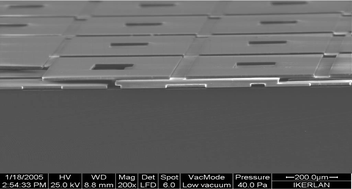
This paper describes a novel fabrication process based on successive wafer-level bonding and releasing steps for stacking several patterned layers of the negative photoresist EPON SU-8. This work uses a polyimide film to enhance previous low temperature bonding technology. The film acts as a temporary substrate where the SU-8 is photopatterned. The poor adhesion between the polyimide film and SU-8 allows the film to be released after the bonding process, even though the film is still strong enough to carry out photolithography. Using this technique, successive adhesive bonding steps can be carried out to obtain complex 3-D multilayer structures. Interconnected channels with smooth vertical sidewalls and freestanding structures are fabricated. Unlike previous works, all the layers are photopatterned before the bonding process yielding sealed cavities and complex three-dimensional structures without using a sacrificial layer. Adding new SU-8 layers reduces the bonding quality because each additional layer decreases the thickness uniformity and increases the polymer crosslinking level. The effect of these parameters is quantified in this paper. This process guarantees compatibility with CMOS electronics and MEMS. Furthermore, the releasing step leaves the input and the output of the microchannels in contact with the outside world, avoiding the usual slow drilling process of a cover. Hence, in addition to the straightforward integration of electrodes on a chip, this fabrication method facilitates the packaging of these microfluidic devices.

You have access to this article
 Please wait while we load your content...
Something went wrong. Try again?


 Please wait while we load your content...