
Mode tunable p-type Si nanowire transistor based zero drive load logic inverter†
Abstract
A design platform for a zero drive load logic inverter consisting of p-channel Si
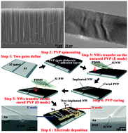
A design platform for a zero drive load logic inverter consisting of p-channel Si
K. Moon, T. Lee, S. Lee, Y. Han, M. Ham and J. Myoung, Chem. Commun., 2012, 48, 7307 DOI: 10.1039/C2CC33818A
To request permission to reproduce material from this article, please go to the Copyright Clearance Center request page.
If you are an author contributing to an RSC publication, you do not need to request permission provided correct acknowledgement is given.
If you are the author of this article, you do not need to request permission to reproduce figures and diagrams provided correct acknowledgement is given. If you want to reproduce the whole article in a third-party publication (excluding your thesis/dissertation for which permission is not required) please go to the Copyright Clearance Center request page.
Read more about how to correctly acknowledge RSC content.
 Please wait while we load your content...

