Metal–insulator–semiconductor field-effect transistors (MISFETs) using p-type SnS and nanometer-thick Al2S3 layers†

Abstract
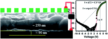
Novel and cost-effective metal–insulator semiconductor field-effect transistor (MISFET) devices were fabricated using non-toxic tin mono sulfide (SnS) as the active layer sandwiched between aluminium and silver contacts with an unintentionally grown aluminium sulfide (Al2S3) interface layer. MISFET devices exhibit a high turn-on voltage of 5.13 V and excellent rectifying diode characteristics. These devices also show a high rectification factor of 1383 at a bias voltage of 6 V and series resistance of 3.4 MΩ, along with a very low leakage current of ∼10−9 A@−10 V. The overall results reveal that it could be possible to fabricate cost-effective and non-toxic MISFET devices by using SnS as an active layer for various power-electronic applications.
 Please wait while we load your content...

