
Study of graphene plasmons in graphene–MoS2 heterostructures for optoelectronic integrated devices†
Abstract
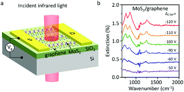
The performance of electronic circuits is becoming limited by on-chip digital information transmission. Graphene plasmons with ultra-high confinement and low damping rates offer an effective solution to this problem as they allow for the implementation of optical interconnects. However, direct contact with the semiconductor always deteriorates the plasmonic properties due to large damping of the plasmon in the semiconductor. Here, we studied graphene plasmons in heterostructures of graphene and monolayer MoS2 which represents a promising semiconductor for next-generation electronic devices. The graphene plasmons in the heterostructures were systematically evaluated in terms of their resonance frequency, intensity, lifetime and electrical tunability and were found to keep their main characteristics. Experimental results exhibited both a redshift in the plasmon frequencies and a decrease in the resonance intensity for both graphene/MoS2 and MoS2/graphene devices when compared with graphene devices at the same gate bias. These results could be attributed to changes in the dielectric constant and effective doping of graphene. Furthermore, the conductivity saturation on the electron branch in the back-gated graphene/MoS2 device cancelled the electron plasmons. These findings demonstrate that electrically tunable graphene plasmons can be realized in contact with semiconducting MoS2. Our results provide a platform for the investigation of the integration of semiconductor-based electronic and optoelectronic devices with plasmonic devices through van der Waals heterostructures.
 Please wait while we load your content...

