
CdS–CdTe heterojunction nanotube arrays for efficient solar energy conversion†
 *a
*a
Abstract
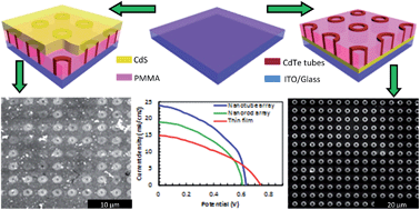
We have established a protocol for the fabrication of CdTe–CdS, lateral p–n junction nanotube arrays, configured akin to either substrate or superstrate geometries. The protocol involves confined electrodeposition of p-type CdTe on lithographically patterned nanoelectrodes defined on conducting substrates, where the substrate surface has been coated with the n-type CdS layer deposited through chemical bath deposition. Post-lithography the underlying CdS layer could be revealed at selective positions, which is the key factor in defining the nature of the formed CdS–CdTe heterojunction. The aspect ratio of the CdTe nanotubes could be controlled by doing pulsed electrodeposition as well as altering the thickness of the polymeric resist used for lithography and tuning the diameter of the nanoelectrodes. Photoelectrochemical analysis in a liquid junction electrolyte has been performed to characterize the photoconductivity response of nanotube arrays. Both the substrate and superstrate p–n junction arrangements of CdS–CdTe nanotube arrays showed photocurrent comparable to that obtained from a bulk film covering a much larger surface area compared to the nanodevice. Typically it was observed that for the heterojunction CdS–CdTe nanotube device less than 10% coverage with the photoabsorber layer was required compared to the bulk film, in order to produce the same amount of photocurrent. Specifically, the photoconversion efficiency was increased by 50% on changing the morphology from bulk film (6.3%) to tubular (9.6%). Additionally, the advantage of the “holey” architecture in the photoabsorber layer was very evident as the photocurrent obtained from the nanotube arrays was larger than that obtained from the nanorod arrays electrodeposited under similar conditions. These observation suggest that these nanotube architectures combining the advantages of both the “holey” and nanopillar geometries might lead to an optimal nanostructured solar cell. The growth method of the nanotube arrays is simple and versatile which can be readily adapted to produce complex photoabsorber layers including the ternary and quaternary chalcogenides.
 Please wait while we load your content...

