Issue 35, 2016

Uncovering the density of nanowire surface trap states hidden in the transient photoconductance

Abstract

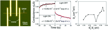
The gain of nanoscale photoconductors is closely correlated with surface trap states. Mapping out the density of surface trap states in the semiconductor bandgap is crucial for engineering the performance of nanoscale photoconductors. Traditional capacitive techniques for the measurement of surface trap states are not readily applicable to nanoscale devices. Here, we demonstrate a simple technique to extract the information on the density of surface trap states hidden in the transient photoconductance that is widely observed. With this method, we found that the density of surface trap states of a single silicon nanowire is ∼1012 cm−2 eV−1 around the middle of the upper half bandgap.

Graphical abstract: Uncovering the density of nanowire surface trap states hidden in the transient photoconductance

Supplementary files

Article information

Article type
Paper
Submitted
22 Jun 2016
Accepted
14 Jul 2016
First published
18 Jul 2016

Nanoscale, 2016,8, 15934-15938

Uncovering the density of nanowire surface trap states hidden in the transient photoconductance

Q. Xu and Y. Dan, Nanoscale, 2016, 8, 15934 DOI: 10.1039/C6NR05014J

To request permission to reproduce material from this article, please go to the Copyright Clearance Center request page.

If you are an author contributing to an RSC publication, you do not need to request permission provided correct acknowledgement is given.

If you are the author of this article, you do not need to request permission to reproduce figures and diagrams provided correct acknowledgement is given. If you want to reproduce the whole article in a third-party publication (excluding your thesis/dissertation for which permission is not required) please go to the Copyright Clearance Center request page.

Read more about how to correctly acknowledge RSC content.

Social activity

Spotlight

Advertisements