Charge transport and mobility engineering in two-dimensional transition metal chalcogenide semiconductors
Abstract
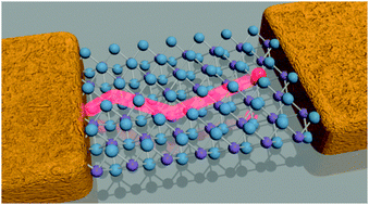
Two-dimensional (2D) van der Waals semiconductors represent the thinnest, air stable semiconducting materials known. Their unique optical, electronic and mechanical properties hold great potential for harnessing them as key components in novel applications for electronics and optoelectronics. However, the charge transport behavior in 2D semiconductors is more susceptible to external surroundings (e.g. gaseous adsorbates from air and trapped charges in substrates) and their electronic performance is generally lower than corresponding bulk materials due to the fact that the surface and bulk coincide. In this article, we review recent progress on the charge transport properties and carrier mobility engineering of 2D transition metal chalcogenides, with a particular focus on the markedly high dependence of carrier mobility on thickness. We unveil the origin of this unique thickness dependence and elaborate the devised strategies to master it for carrier mobility optimization. Specifically, physical and chemical methods towards the optimization of the major factors influencing the extrinsic transport such as electrode/semiconductor contacts, interfacial Coulomb impurities and atomic defects are discussed. In particular, the use of ad hoc molecules makes it possible to engineer the interface with the dielectric and heal the vacancies in such materials. By casting fresh light on the theoretical and experimental studies, we provide a guide for improving the electronic performance of 2D semiconductors, with the ultimate goal of achieving technologically viable atomically thin (opto)electronics.


 Please wait while we load your content...