
Effect of hydrogen in controlling the structural orientation of ZnO:Ga:H as transparent conducting oxide films suitable for applications in stacked layer devices
Abstract
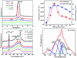
Hydrogenation of the ZnO:Ga network has been chosen as a promising avenue to further upgrade the optoelectronic and structural properties of the films. With an optimum incorporation of hydrogen at a low substrate temperature (TS = 100 °C) in RF magnetron sputtering plasma, the ZnO:Ga:H film, with a large crystallite size (∼17 nm) and improved crystallinity along the optimally preferred c-axis orientation with respect to both the 〈100〉 (I〈002〉/I〈100〉 ∼ 74) and 〈103〉 (I〈002〉/I〈103〉 ∼ 10) directions, attains a high electrical conductivity (σ ∼ 1.5 × 10³) and ∼90% visible range optical transmission that yields a wide optical band gap of ∼3.78 eV. The dominant c-axis orientation of the ZnO crystals exhibits a distinct UV luminescence band at ∼340 nm that arises as a result of the typical exciton emission or near-band-edge emission, which occurs due to the recombination of photo-generated electrons and holes in the valence band or in traps near the valence band. Vacancies created by the out diffusion of oxygen from the network induces the growth along the 〈103〉 crystallographic orientation. With the introduction of an optimum amount of hydrogen into the network, the VO peak (OII) in the O 1s XPS spectrum significantly reduces in intensity while the Zn–OH peak (OIII) increases, indicating enhanced surface absorption of O species, which causes the improvement of c-axis orientation. The increase in the conductivity has been attributed to the centers assigned to isolated hydrogen atoms in the anti-bonding sites (ABO) or bond-centered sites of O–Zn bonds (BC), and Zn vacancies passivated by one or two hydrogen atoms. Hydrogen-induced dopant-like defects in the film and the associated large amount of tensile stress developed within the network has been correlated to the high conductivity and the wide band gap of the ZnO:Ga:H film due to the decreased repulsion between the O 2p and the Zn 4s bands and the Burstein–Moss effect as a consequence of the increased carrier concentration. Highly conducting and transparent c-axis oriented ZnO:Ga:H films grown by a device compatible process at a low TS are extremely useful for various stacked layer thin film devices, including solar cells.
 Please wait while we load your content...

