Issue 6, 2015

The effect of strain on the electrical conductance of p-type nanocrystalline silicon carbide thin films

Abstract

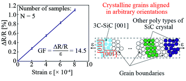
This paper presents for the first time the effect of strain on the electrical conductance of p-type nanocrystalline SiC grown on a Si substrate. The gauge factor of the p-type nanocrystalline SiC was found to be 14.5 which is one order of magnitude larger than that in most metals. This result indicates that mechanical strain has a significant influence on the electrical conductance of p-type nanocrystalline SiC, which is promising for mechanical sensing applications in harsh environments.

Graphical abstract: The effect of strain on the electrical conductance of p-type nanocrystalline silicon carbide thin films

Article information

Article type
Communication
Submitted
24 Nov 2014
Accepted
26 Dec 2014
First published
08 Jan 2015

J. Mater. Chem. C, 2015,3, 1172-1176

Author version available

The effect of strain on the electrical conductance of p-type nanocrystalline silicon carbide thin films

H. Phan, D. V. Dao, L. Wang, T. Dinh, N. Nguyen, A. Qamar, P. Tanner, S. Dimitrijev and Y. Zhu, J. Mater. Chem. C, 2015, 3, 1172 DOI: 10.1039/C4TC02679A

To request permission to reproduce material from this article, please go to the Copyright Clearance Center request page.

If you are an author contributing to an RSC publication, you do not need to request permission provided correct acknowledgement is given.

If you are the author of this article, you do not need to request permission to reproduce figures and diagrams provided correct acknowledgement is given. If you want to reproduce the whole article in a third-party publication (excluding your thesis/dissertation for which permission is not required) please go to the Copyright Clearance Center request page.

Read more about how to correctly acknowledge RSC content.

Social activity

Spotlight

Advertisements