Coplanar homojunction a-InGaZnO thin film transistor fabricated using ultraviolet irradiation
Abstract
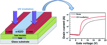
We have developed a new technique to fabricate coplanar homojunction structure a-IGZO thin film transistors (TFTs) by adopting selective ultraviolet (UV) irradiation in the n+ source/drain regions of an a-IGZO layer through a patterned photoresist mask. In order to apply this technique for coplanar homojunction a-IGZO TFTs, we systematically studied the effect of dual wavelength (185 nm and 254 nm) UV irradiation time on the conductivity of a-IGZO films. Various materials were evaluated to find one that provided proper shielding against UV irradiation. The resistivity of the a-IGZO film drastically decreased from an as-deposited value of 2.71 × 10⁶ Ω cm to 3.76 × 10⁻⁵ Ω cm after UV irradiation. The lowest resistivity obtained in this study is similar to that of ITO transparent electrodes and is about 2 orders of magnitude lower than the values obtained to date. Coplanar homojunction a-IGZO TFTs were successfully fabricated by introducing an optimized process that included UV irradiation through a patterned photoresist UV mask. The saturation mobility (μsat), threshold voltage (Vth), sub-threshold swing (SS), and on/off current ratio (Ion/Ioff) were measured to be 6.7 cm2 V−1 s, 7.3 V, 0.21 V per decade, and ∼109, respectively. Moreover, we showed that the UV irradiation technique provided both a low contact resistance due to the high conductivity in the source/drain region and a small channel length modulation due to non-thermal doping behavior. We believe that this UV irradiation process is a useful technique because it is simple and results in outstanding electrical properties.
 Please wait while we load your content...

