
High-yield fabrication of nm-size gaps in monolayer CVD graphene†
Abstract
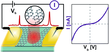
Herein we demonstrate the controlled and reproducible fabrication of sub-5 nm wide gaps in single-layer graphene electrodes. The process is implemented for graphene grown via chemical vapor deposition using an electroburning process at room temperature and in vacuum. A yield of over 95% for the gap formation is obtained. This approach allows producing single-layer graphene electrodes for molecular electronics at a large scale. Additionally, from Raman spectroscopy and electroburning carried out simultaneously, we can follow the heating process and infer the temperature at which the gap formation happens.
 Please wait while we load your content...

