Issue 38, 2013

Van der Waals epitaxial growth of MoS2 on SiO2/Si by chemical vapor deposition

Abstract

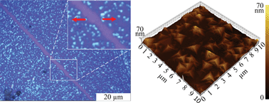
Recently, single layer MoS2 with a direct band gap of 1.9 eV has been proposed as a candidate for two dimensional nanoelectronic devices. However, the synthetic approach to obtain high-quality MoS2 atomic thin layers is still problematic. Spectroscopic and microscopic results reveal that both single layers and tetrahedral clusters of MoS2 are deposited directly on the SiO2/Si substrate by chemical vapor deposition. The tetrahedral clusters are mixtures of 2H- and 3R-MoS2. By ex situ optical analysis, both the single layers and tetrahedral clusters can be attributed to van der Waals epitaxial growth. Due to the similar layered structures we expect the same growth mechanism for other transition-metal disulfides by chemical vapor deposition.

Graphical abstract: Van der Waals epitaxial growth of MoS2 on SiO2/Si by chemical vapor deposition

Article information

Article type
Paper
Submitted
02 May 2013
Accepted
19 Jul 2013
First published
22 Jul 2013

RSC Adv., 2013,3, 17287-17293

Van der Waals epitaxial growth of MoS2 on SiO2/Si by chemical vapor deposition

Y. Cheng, K. Yao, Y. Yang, L. Li, Y. Yao, Q. Wang, X. Zhang, Y. Han and U. Schwingenschlögl, RSC Adv., 2013, 3, 17287 DOI: 10.1039/C3RA42171F

To request permission to reproduce material from this article, please go to the Copyright Clearance Center request page.

If you are an author contributing to an RSC publication, you do not need to request permission provided correct acknowledgement is given.

If you are the author of this article, you do not need to request permission to reproduce figures and diagrams provided correct acknowledgement is given. If you want to reproduce the whole article in a third-party publication (excluding your thesis/dissertation for which permission is not required) please go to the Copyright Clearance Center request page.

Read more about how to correctly acknowledge RSC content.

Social activity

Spotlight

Advertisements