
As flat as it gets: ultrasmooth surfaces from template-stripping procedures
Abstract
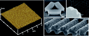
In an experimentally simple replica process, the natural flatness of mica or polished silicon wafers can be transferred to metal films, resulting in metal surfaces with topographic features in Angstrom dimensions over large areas. Two decades after its invention, the template-stripping process continues to appeal to scientists from diverse research backgrounds primarily due to its simplicity, cost-effectiveness and ability to yield high quality substrates and structures. This article introduces the basic construction process for template-stripped substrates, and reports on a variety of extensions of the process, including the generation of materials contrasts and the design of tailored topographies. It also highlights the use of such substrates in a variety of research fields in nanoscience and technology ranging from surface force measurement and high definition imaging to the self-assembly of model membranes and plasmonics.
 Please wait while we load your content...

