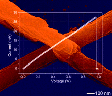
Growth of silver nanowires on GaAs wafers†
Abstract
Silver (Ag)

Maintenance work is planned for Wednesday 1st May 2024 from 9:00am to 11:00am (BST).
During this time, the performance of our website may be affected - searches may run slowly and some pages may be temporarily unavailable. If this happens, please try refreshing your web browser or try waiting two to three minutes before trying again.
We apologise for any inconvenience this might cause and thank you for your patience.
* Corresponding authors
a
Center for Nanoscale Materials, Argonne National Laboratory, 9700 South Cass Avenue, Argonne, Illinois, USA
E-mail:
ygsun@anl.gov
Fax: +1-630-252-4646
Tel: +1-630-252-3716
Silver (Ag)

 Please wait while we load your content...
Something went wrong. Try again?
Y. Sun, Nanoscale, 2011, 3, 2247 DOI: 10.1039/C1NR10153F
To request permission to reproduce material from this article, please go to the Copyright Clearance Center request page.
If you are an author contributing to an RSC publication, you do not need to request permission provided correct acknowledgement is given.
If you are the author of this article, you do not need to request permission to reproduce figures and diagrams provided correct acknowledgement is given. If you want to reproduce the whole article in a third-party publication (excluding your thesis/dissertation for which permission is not required) please go to the Copyright Clearance Center request page.
Read more about how to correctly acknowledge RSC content.
 Fetching data from CrossRef.
This may take some time to load.
Loading related content
