
From stochastic single atomic switch to nanoscale resistive memory device†
Abstract
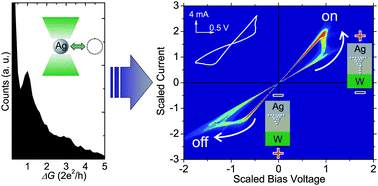
We study the switching characteristics of nanoscale junctions created between a tungsten tip and a silver film covered by a thin ionic conductor layer. Atomic-sized junctions show spectacular current induced switching characteristics, but both the magnitude of the switching voltage and the direction of the switching vary randomly for different junctions. In contrast, somewhat larger junctions with diameters of a few nanometres display a well defined, reproducible switching behavior attributed to the formation and destruction of nanoscale channels in the ionic conductor surface layer. Our results define a lower size limit of 3 nm for reliable ionic nano-switches, which is well below the resolution of recent lithographic techniques.
 Please wait while we load your content...

