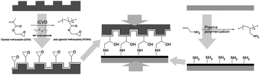
A novel high-strength nano-adhesive is demonstrated for fabricating nano- and microfluidic devices. While the traditional plasma sealing methods are specific for sealing glass to poly(dimethylsiloxane) (PDMS), the new method is compatible with a wide variety of polymeric and inorganic materials, including flexible substrates. Additionally, the traditional method requires that sealing occur within minutes after the plasma treatment. In contrast, the individual parts treated with the nano-adhesive could be aged for at least three months prior to joining with no measurable deterioration of post-cure adhesive strength. The nano-adhesive is comprised of a complementary pair of polymeric nanolayers. An epoxy-containing polymer, poly(glycidyl methacrylate) (PGMA) was grown via initiated chemical vapor deposition (iCVD) on the substrate containing the channels. A plasma polymerized polyallylamine (PAAm) layer was grown on the opposing flat surface. Both CVD monomers are commercially available. The PGMA nano-adhesive layer displayed conformal coverage over the channels and was firmly tethered to the substrate. Contacting the complementary PGMA and PAAm surfaces, followed by curing at 70 °C, resulted in nano- and micro-channel structures. The formation of the covalent tethers between the complementary surfaces produces no gaseous by-products which would need to outgas. The nano-adhesive layers did not flow significantly as a result of curing, allowing the cross-sectional profile of the channel to be maintained. This enabled fabrication of channels with widths as small as 200 nm. Seals able to withstand > 50 psia were fabricated employing many types of substrates, including silicon wafer, glass, quartz, PDMS, polystyrene petri dishes, poly(ethylene terephthalate) (PET), polycarbonate (PC), and poly(tetrafluoro ethylene) (PTFE).

 Please wait while we load your content...

