
Strongly-coupled PbS QD solids by doctor blading for IR photodetection†
Alberto Maulua,
Pedro J. Rodríguez-Cantó*b,
Juan Navarro-Arenas a,
Rafael Abarguesb,
Juan F. Sánchez-Royoa,
Raúl García-Calzadaa and
Juan P. Martínez Pastor*a
a,
Rafael Abarguesb,
Juan F. Sánchez-Royoa,
Raúl García-Calzadaa and
Juan P. Martínez Pastor*a
aInstituto de Ciencia de los Materiales, Universidad de Valencia, P. O. Box 22085, 46071 Valencia, Spain
bINTENANOMAT S.L., C/Catedrático José Beltrán 2, 46980 Paterna, Spain. E-mail: pedro.j.rodriguez@uv.es
First published on 8th August 2016
Abstract
Solution-processed QD solids are emerging as a novel concept for high-performance optoelectronic devices. In this work, doctor blading is proposed for the fabrication of strongly-coupled QD solids from a PbS nanoink for photodetection at telecom wavelengths. The key step of this procedure is the solid-state ligand exchange, which reduces the interparticle distance and increases the carrier mobility in the resulting strongly-coupled QD solid. This is accomplished by replacing the original long oleylamine molecules by shorter molecules like 3-mercaptopropionic acid, as confirmed by FTIR, TGA and XPS. Further, a detailed investigation with XPS confirms the air-stability of the QD solids and the extreme reduction of the principal oxidation product, PbSO3, from ligand exchange times of 60 s. Finally, the QD solid is tested as an active layer for the fabrication of a Schottky NIR photodetector. The device shows a maximum responsivity of 0.26 A W−1 that corresponds to an internal quantum efficiency higher than 30% at 1500 nm and detectivity around 1011 jones.
Introduction
Quantum dots (QDs) have been proved to be promising materials for the development of optoelectronic devices for photovoltaics,1–5 light emitting diodes,6–8 and photodetection,9–15 because of their unique electronic and optical properties. These properties include band gap tunability, strong absorption and emission over a wide range of energies, high photoluminescence quantum yield and narrow emission line width. Moreover, they can be synthesized with different capping agents to form colloidal solutions, as the basis to be processed in the form of self-assembled solid-state materials using low-cost and large-area deposition techniques. However, the efficient transfer of QDs from solution to solid-state is a major technological challenge in order to develop efficient QD-based optoelectronic devices, while maintaining the three-dimensional confinement of the nanocrystals and hence the properties highlighted above for QDs. The use of colloidal QDs as building blocks to form self-assembled QD “super-crystals” with low defect concentration and high mobility is thus considered an advanced concept for optoelectronic devices.The synthesis of colloidal QDs with uniformity in composition, size and shape together with their surface functionalization with adequate capping agents are essential requirements to control the QD assembly and the interparticle distance within the QD film to obtain close-packed QD solids with high mobility and Bloch electronic transport of carriers.16 Specially, the formation of well-ordered QD self assemblies paves the road to novel collective properties due to electronic coupling between individual QDs. However, the application of QD solids in optoelectronic devices has been hindered by the lack of a suitable and low-cost, solution-based deposition method for the fabrication of well-ordered assemblies on large areas.17
To date, deposition techniques such spray- or dip-coating are often used to form large-area QD solids from colloidal solutions.18 The success of these coating technologies relies on their simplicity, versatility, and the accurate control of the film thickness, other than the possibility to use different substrates. Nevertheless, they lead to fast evaporation rates resulting in amorphous and glassy QD solids. Other deposition techniques, such as simple drop casting,19 Langmuir–Blodgett technique,20 and spin coating,21 are more adequate to obtain ordered QD films, but typically present some disadvantages. Whereas drop casting is usually appropriate for small deposition areas, in the order of centimetre, the Langmuir–Blodgett technique requires long times between each deposited layer to obtain thick films. Besides, spin coating allows for the coating of larger areas but it is time-consuming and leads to vast material waste (only a 1–10% of coated QD solution is incorporated into the film).22 Therefore, none of these techniques are ideal to form thick QD solids that are required to typically produce high-performance absorber layers in optoelectronics devices.
A very promising coating technique is doctor blading, which basically uses a coating blade to apply a solution uniformly over the substrate. The resulting thickness can be properly varied by simply adjusting the gap height and width between the blade and the substrate, the temperature of the substrate, the blading speed as well as the ink properties. This method allows for the coating of large areas with a small waste of material and an accurate control on the film thickness. Moreover, it improves the coating performance by the control of the surface tension and wetting properties of the solution to the substrate.15 This technique also takes advantage of the relatively large choice of organic solvents available and the possibility of transfer to roll-to-roll knife coating.23 The application of this deposition technique can be found, for example, in the manufacturing of printed bulk heterojunction solar cells and QD-sensitized organic infrared photodiodes, whose performances are similar to those processed by spin coating.24,25 Further, this deposition technique has been also used to form large-area ordered magnetic nanocrystal thin films, resulting in a degree of ordering that outperforms those provided by alternative deposition techniques such as inkjet printing or drop casting.14 Nevertheless, to the best of our knowledge, this technique has not been applied to form solution-processable QD solids so far.
In the present work, we demonstrate the use of the doctor blading technique for the fabrication of QD solids from a solution-processable PbS QD nanoink for photodetection at telecom wavelengths. The application of QD solids for the fabrication of photodetectors is receiving steadily growing attention, given the strong absorption of the QDs at the band edge, the size-tunable bandgap, surface chemistry and the possibility to manufacture devices using inexpensive QD inks.26 Among the different types of QD materials, PbS is a very promising semiconductor material since it possesses a direct narrow band gap (0.41 eV) and a large exciton Bohr radius (18 nm). As a result, its optical properties can be tuned from the infrared to the visible allowing for the development of multispectral photodetectors.27 In the literature, some works on PbS QD photodetectors can be recently found. Clifford et al.28 reported a photodetector architecture based on a 350 nm thick PbS film produced by spin coating that reached a responsivity of 0.2 A W−1 (EQE of 17–25% at 1450 nm over a bias range 0.0 to 21.0 V). Moreover, Pal et al.29 achieved EQE values up to 80% at different wavelengths ranging from 450 to 1000 nm with a p–n junction architecture consisting in a oxide layer as n-type material and a PbS QD layer as p-type fabricated by spin coating. In this work, we propose the use of doctor blading for the fabrication of smooth, close-packed solids from a PbS QD nanoink. The QDs are capped with oleyamine (OAm) because this large molecule (∼3.6 nm) would promote a direct self-assembly of QDs once the nanoink is deposited onto a substrate. Afterwards, we carry out a solid-state ligand exchange to reduce the interparticle distance and increase the carrier mobility in the QD solid, other than promoting the surface passivation of QDs and, consequently, improving the carrier diffusion length. Here, we choose 3-mercaptopropionic acid (MPA) as short bidentate ligand because it offers an improved passivation of our PbS QDs and leads to an increase in the mobility-lifetime product as well as an enhancement of the minority carrier transport.30 Given that the ligand exchange is the key step on the fabrication of high performance photodevices, we thoroughly characterized it by FTIR, TGA and XPS. A detailed investigation by XPS of the resulting QD solids before and after the ligand exchange was conducted to investigate the surface state and stability. Finally, as a proof of concept, the QD solid produced by doctor blading has been used as the active layer of a Schottky-heterostructure photodiode operating at telecom wavelengths. Despite the relative simple architecture of the photodiode, we measured a maximum responsivity (R) of 0.26 A W−1 corresponding to an internal quantum efficiency (IQE) higher than 30% at 1500 nm, detectivity D* ≈ 1011 jones and response time around 135 μs. These values are comparable to those achieved in similar architectures fabricated by using the standard layer-by-layer spin coating.24–26 These results demonstrate that solution-processed QD solids fabricated by roll-to-roll compatible doctor blading deposition technique might be the basis for the development of cost-effective and large area optoelectronic devices, as photodetectors and solar cells.
Experimental
Materials
Sulfur (99.999%, S), lead chloride (99.999%, PbCl2), 3-mercaptopropionic acid (≥99%, MPA), poly(3,4-ethilenedioxythiophene)–poly(styrenesulfonate) (1.1% H2O, PEDOT:PSS) were purchased from Sigma-Aldrich. Oleylamine (OAm), methanol and octane were all of quality “for synthesis”.Synthesis of PbS QD nanoink
We synthesize PbS QDs according to the procedure described by Cademartiri et al.31 The ratio of Pb![[thin space (1/6-em)]](https://www.rsc.org/images/entities/char_2009.gif) :S was set to 3:1. Firstly, a solution of 0.05 g of S (1.5 mmol) dissolved in 5 mL of OAm is prepared by heating the mixture under N2 at 125 °C for 60 min. In a typical synthesis, 1.4 g of PbCl2 (5 mmol) and 15 mL of OAm were degassed under N2 in a three-neck flask at 125 °C for 60 min, which produced a clear solution of lead oleate. Afterward, the solution was heated up to 130 °C and the S precursor solution was swiftly injected into the reaction flask. The reaction was maintained for 7 min to obtain the required QD size. Then, the PbS solution was slowly cooled and washed twice by suspending in toluene and precipitating with methanol. In the final step, the PbS QDs were dispersed in octane at a concentration of 150 mg mL−1, which was found to be the optimal concentration to formulate the QD nanoink.
:S was set to 3:1. Firstly, a solution of 0.05 g of S (1.5 mmol) dissolved in 5 mL of OAm is prepared by heating the mixture under N2 at 125 °C for 60 min. In a typical synthesis, 1.4 g of PbCl2 (5 mmol) and 15 mL of OAm were degassed under N2 in a three-neck flask at 125 °C for 60 min, which produced a clear solution of lead oleate. Afterward, the solution was heated up to 130 °C and the S precursor solution was swiftly injected into the reaction flask. The reaction was maintained for 7 min to obtain the required QD size. Then, the PbS solution was slowly cooled and washed twice by suspending in toluene and precipitating with methanol. In the final step, the PbS QDs were dispersed in octane at a concentration of 150 mg mL−1, which was found to be the optimal concentration to formulate the QD nanoink.
QD solid fabrication
The QD solids were fabricated by doctor blading in air. Briefly, the ITO substrates were cleaned by rinsing in isopropanol and water and dried under N2 flow. Then, PEDOT:PSS was cast onto the ITO coated glass substrate using a commercial Doctor Blade film applicator (Elcometer 4340) and subsequently annealed at 110 °C for 5 min. For each PbS QD layer, 12 μL of the PbS QD solution (150 mg mL−1 in octane) were applied in the gap between the substrate and the blade. Afterwards, the blade was moved along the substrate with a velocity of 1.5 cm s−1 and the sample was baked at 100 °C for 5 min. This cycle was repeated seven times, resulting in a film thickness of around 450 nm. Finally, the sample was annealed at 100 °C for 1 h under vacuum.For the ligand exchange, the sample was dipped in a solution of MPA in methanol (10 vol%) for different times, rinsed with methanol to remove the MPA excess, dried under N2 flow, and annealed at 100 °C under vacuum for 1 h. Finally, 100 nm thick Ag electrodes were thermally deposited using an aluminum foil as a shadow mask. In order to protect the electrodes against the oxidation, we encapsulated them with a silicone layer.
Characterization
X-ray diffraction (XRD), low-angle XRD, and grazing incidence diffraction (GID or GIXD) patterns of the QD film deposited on glass were recorded by a Brucker D8 Advance X-ray diffractometer using Cu Kα radiation (λ = 0.15406 nm). The average size of the PbS QDs was determined from the broadening of XRD peaks by using the Scherrer formula.High-resolution transmission electron microscopy (HRTEM) images and EDX characterization were carried out using a field-emission gun (FEG) TECNAI G2 F20 microscope (from FEI) operated at 200 kV. The morphology and thickness of thin QD films were determined by cross-section and surface SEM through a Hitachi 4800 microscope.
X-ray photoelectron spectroscopy (XPS) measurements were performed in an ultrahigh vacuum system ESCALAB-210 (base pressure 1.0 × 10⁻¹⁰ mbar) from Thermo VG Scientific. Photoelectrons were excited using the Mg Kα line (1253.6 eV) and the measurements were taken over an area of 1 mm2. As a reference in the binding energy, the C 1s peak was used (fixed to 285 eV).
Thermogravimetric analysis of powder made from the QD solids was performed by using a Setaram Setsys 16/18 TG-DTA instrument. To prepare the samples, the QD solids were scratched off the substrates to obtain about 5 mg of material. The samples were heated from 30 to 300 °C under a O2 flow at a heating rate of 10 °C min−1.
Fourier transform infrared spectroscopy (FTIR) was performed on a Bruker Tensor spectrometer in transmission mode. KBr disks were used for all measurements.
The electro-optical properties of the photodetector in the infrared region (>1100 nm) were measured by an in-house set-up based on a halogen lamp (20 W) focused into an optical fiber attached to the entry of a DeltaNu DNS-300 monochromator with 600 grooves per mm grating blazed at 1200 nm, whose output was modulated at 1 kHz by means of a mechanical chopper and focused onto the fabricated photodetector by a 10× objective; the electrical signal of the photodetector was synchronously measured by a lock-in amplifier. The incident power to the samples as a function of the wavelength at the monochromator output was measured using a Newport's DET-L-GE-T-C calibrated Ge photodetector. Responsivity was calculated by comparison with the calibrated table of this Ge photodetector. Intensity–voltage characteristics under dark and illumination conditions were measured using a Keithley's Series 2400 Source Measure Unit (SMU). Capacitance–frequency and capacitance–voltage measurements were performed using a LCR Meter model 1920.
Results and discussion
Synthesis and characterization of the colloidal PbS QD nanoink
Nanoinks containing QDs with uniformity in composition, size, shape, and surface passivation have been optimally formulated to form dense QD solids with high mobility suitable for high-performance optoelectronic devices, such as photodetectors. PbS is a narrow gap semiconductor with a bulk band gap of 0.41 eV and an exciton Bohr radius of 18 nm. As a result, its optical properties can be easily tuned over practically the entire NIR spectral range by simply adjusting the QD size during the synthesis. Because QD inks can be processed from solution and show tunable optical properties, they are suitable materials for multispectral devices, which may be compatible with silicon technology. The synthesis of colloidal PbS QDs developed in this work uses lead chloride (PbCl2) and elemental sulfur (S) as precursors and oleylamine (OAm) as coordinating solvent, which simultaneously acts as ligand and solvent. The use of PbCl2 as metal precursor may greatly enhance the QD stability in suspension since introduces ions (Cl−) that have demonstrated passivation of QD trap states and effectively prevention of surface oxidation over time in solution. This elemental sulfur-based synthetic route firstly reported by Cademartiri et al.31 has been optimized in the present work to produce large PbS nanocrystals of around 6–7 nm in diameter to develop nanoinks for doctor blading QD solids. Fig. 1a shows a well-defined excitonic peak in absorption centred at 1500 nm with a full width at half-maximum (FWHM) of 140 nm, whereas the corresponding photoluminescence (PL) band is located at 1550 nm with a FWHM of 130 nm. | ||
| Fig. 1 (a) Absorbance (blue line) and photoluminescence (red line) spectra of the as-synthesized PbS QDs in octane. (b) TEM image of spherical PbS QDs. Inset: size histogram. The mean size equals 6.7 nm, with a size dispersion of 8.5%. (c) HRTEM image of a PbS QD showing crystallinity and absence of lattice defects. (d) HRTEM-SAED image showing a diffraction of crystal planes consistent with PbS bulk lattice parameters. (e) GIXD pattern of the PbS QDs deposited on glass. The vertical blue lines indicate the diffraction peaks of bulk PbS (JCPDS 02-0699). | ||
During the synthesis we used OAm as coordinating solvent because of two reasons mainly. Firstly, OAm leads to a viscose suspension with decreased mass-transfer coefficient that allows for a more diffusion-controlled growth of QDs. Secondly, OAm facilitates an efficient ligand exchange during the device fabrication. The OAm coordinates the surface Pb atoms through the nitrogen lone pair electrons of the amine, which results in a weaker bond than that of, for instance, the carboxylic group of the oleic acid. Then, the dynamic nature of OAm capping will allow for a fast and efficient solid-state ligand exchange during device fabrication without compromising the stability of the QDs in solution. Fig. S1† compares the emission spectrum of a freshly prepared PbS QD solution before and after two months. As can be observed, only a small shift could be noticed indicating that the solution is quite stable.
The average size of the PbS QDs was determined by transmission electron microscopy (TEM) measurements. Fig. 1b shows a TEM image of the spherical PbS nanocrystals with an average size of 6.7 nm and a relative size dispersion σd = 8.5% (inset of Fig. 1b). This size is in good agreement with that determined on the basis of the energy of the PbS ground exciton energy (Fig. 1a) from well-known empirical formulas.32 High-resolution transmission electron microscopy (HRTEM) image (Fig. 1c) suggests that the nanocrystals are highly crystalline and free from stacking faults and lattice defects. The selected area electron diffraction (SAED) pattern (Fig. 1d) is consistent with the rock salt structure of bulk PbS material. Furthermore, the lattice d-spacing of the PbS nanocrystal shown in Fig. 1d was estimated to be 0.30 nm, which is in good agreement with the (200) lattice plane for bulk PbS (JCPDS card no. 02-0699). The composition of the PbS core was analysed by energy-dispersive X-ray spectroscopy (EDX) (Fig. S2a†). Pb and S are observed in the pattern (carbon and copper signals come from the carbon-coated copper grids), with a Pb:S ratio 55:45.
Fig. 1e shows the grazing incidence X-ray diffraction (GIXD) patterns of a 400 nm thick PbS film prepared on glass by doctor blading and cured at 110 °C for 10 min. The analysis of these patterns in PbS nanocrystals forming the QD solid correspond to the PbS bulk with rock salt crystal structure. The diffraction peaks at 2θ = 25.8°, 29.9°, 42.9°, 50.9°, 53.3°, 62.5°, 68.8°, 70.8°, and 78.9° are well matched with (111), (200), (220), (311), (222), (400), (331), (420) and (422) crystalline planes of cubic phase (galena) of PbS (JCPDS card no. 02-0699). Furthermore, the absence of significant peaks at 22.9°, 35.8°, and 46.5° in the GIXD pattern as well as in the XRD (Fig. S2b†) indicates a negligible presence of PbCl2 after the synthesis and purification. We determined a lattice constant of 0.5957 nm, comparable to the standard value of 0.5936 nm for bulk PbS. Moreover, the average diameter of the QDs in the thin film was estimated to be ≈6.7 nm, i.e., similar to the value extracted from TEM images, as deduced from the Debye–Scherrer formula33 applied to the linewidth of the (200) in GIXD and XRD patterns (Fig. 1e and S2b†).
Fabrication and characterization of the PbS QD solid by doctor blading
In this work, we propose the use of a doctor blading deposition technique that provides fast and highly efficient utilization of colloidal QD inks and enable large-area deposition in a single or several deposition steps. The desired final thickness of the QD solid is a result of the QD nanoink properties as well as the blading parameters such as the slit height between the substrate and the knife, the volume of the QD solution applied in the slit, and the blading speed. This fabrication process allows an accurate control of the surface tension and wetting properties of the colloidal solution relative to the underlying substrate,15 added to the advantage of a large choice of organic solvents that can be used for the ink formulation. One important aspect of this simple technique is that the processing time is significantly reduced compared to that required in other conventional coating techniques. Furthermore, doctor blading is capable of achieving thicker high-compact films in a reproducible and controllable way. The doctor blading approach is schematically depicted in Fig. 2a and has been carried out under ambient conditions. | ||
| Fig. 2 (a) Schematic illustration of the fabrication process of the QD solids by doctor blading. (b) Low- and high resolution TEM images of a self-assembled monolayer of OAm-capped PbS QDs. (c) Low- and high resolution SEM images of the PbS QD solid surface. The removal of OAm ligands by MPA does not cause significant morphological defects such as cracking or pinholes within the film. | ||
As starting material, we have formulated the nanoink with highly monodisperse (σd = 8.5%) OAm-capped PbS QDs in octane. The doctor blade coating is mainly determined by an adequate nanoink formulation. Functional inks must accomplish some rheological requirements such as the surface tension, which is the most important parameter.34,35 This will be responsible for the ink wetting properties on the substrate, homogeneity of the film and the suppression of “coffee ring effect”.36–38 We found an optimum formulation of the QD-nanoink with a QD concentration of 150 mg mL−1 in octane that exhibits a surface tension of 36 dyn cm−1 and a contact angle on the PEDOT layer of ≈7°. Octane is a suitable solvent because the drying rate of the wet film processed by doctor blading allows sufficient time for the QDs on the surface to find equilibrium “super-lattice” sites, leading to an optimal self-assembly of QDs into a close-packed superlattice,39 as observed in Fig. 2b and c. The films are formed by dropping 12 μL of the PbS QD nanoink in the gap between the substrate and the blade. This gap was adjusted to 2 mm for all experiments. Then, the blade is moved along the substrate with a velocity of 1.5 cm s−1 to uniformly spread the solution over the whole sample area. Finally, the sample is baked at 100 °C for 5 min to completely remove the solvent.
The OAm long ligands give rise to large interparticle distances that leads to very weak electronic coupling between neighbouring QDs, i.e., extremely low Bloch (band-like) mobility.13 In fact, resistivity values >1010 ohm cm were measured in OAm-capped PbS QD films. In order to produce QD solids with much lower resistivity, it is necessary to chemically exchange the original OAm ligands by shorter or conjugated organic molecules such as alkyl and aryl mono- and dithiolates, isocyanates, amines and acids,40 or inorganic ligands such as hydrazine,41 chalcogenidometallates,42 halometallates,43 chalcogenides,44 halides45 and pseudohalides.46 Such a ligand exchange leads to both the increase of electronic coupling between neighbouring QDs by reducing the interparticle spacing and an efficient passivation. In this work, we have chosen MPA as short bidentate ligand because it offers improved passivation of the PbS QDs and leads to an increase in the mobility-lifetime product as well as an enhancement of the minority carrier transport. Furthermore, the density and energetic distribution of defect energy levels below the conduction band are reduced in comparison to other organic molecules.27 The ligand exchange has been carried out by immersing the OAm-capped PbS QD film in a solution of MPA in methanol (10 vol%). Owing to the high affinity of the thiol group of MPA for the Pb2+ metal cation sites on the QD surfaces, the OAm ligand was efficiently displaced by MPA. As a consequence, the resulting resistivity of the QD solid after the ligand exchange is reduced by around five orders of magnitude (ρ ≈ 105 Ω cm, as measured using ohmic contacts on a 500 nm thick QD-solid deposited on glass). Fig. S3† shows a photograph of the QD solid produced by doctor blading on a 7.5 × 2.5 cm2 substrate.
The TEM images shown in Fig. S4† reveal the decrease in the average spacing after the MPA treatment. Using image analysis, we determine the average center-to-center distance to be 9.0 ± 0.7 nm before the ligand exchange and 7.4 ± 0.5 nm after the MPA passivation. These values are consistent with the low angle X-ray diffraction patterns measured in MPA- and OAM-capped PbD QD-films (see Fig. S5a†), which result from the self-organization of the QDs into a body-centered cubic (BCC) superlattice. From both experiments, TEM and low-angle XRD, we estimate the interparticle separation of OAm-capped PbS QDs to be around 2.3–2.4 nm, which is significantly reduced to 0.7–1.1 nm after the ligand exchange.
Generally speaking, the main problem of using a solid-state ligand exchange is the typical formation of morphological defects in the thin film, which may result in low efficiency and inconsistent performance of the device. In spite of this a priori inconvenience, the PbS QD solids produced by doctor blading exhibit crack-free and homogeneous films even after ligand exchange (Fig. 2c). Thereby, this technique is suitable for producing dense and pinhole-free QD solids from properly formulated nanoinks for the fabrication of optoelectronic devices with good overall performance, as demonstrated below in the case of a Schottky-heterostructure photodetector at telecom wavelength.
The solid-state ligand exchange is confirmed by Fourier transform infrared spectroscopy (FTIR). The exchange of OAm by MPA in QD films is clearly observed by the loss of the C![[double bond, length as m-dash]](https://www.rsc.org/images/entities/char_e001.gif) C stretching vibration peak at 3005 cm−1 and the strong decrease in intensities of the aliphatic C–H stretching peaks at 2845–2915 cm−1, as observed in Fig. 3a. Moreover, the symmetric and asymmetric stretching vibrations of the carboxylate group of MPA appear at 1380 and 1510 cm−1, respectively, and the N–H bending vibration at 1550 cm−1 is not observed after the ligand exchange. The absence of S–H bond stretching vibration modes in the region 2500–2600 cm−1 suggests that any excess of free MPA has been completely removed after washing with methanol. Thus, the binding of MPA to PbS is accomplished through chemical bonding between thiols and free coordination sites on Pb(II) atoms.
C stretching vibration peak at 3005 cm−1 and the strong decrease in intensities of the aliphatic C–H stretching peaks at 2845–2915 cm−1, as observed in Fig. 3a. Moreover, the symmetric and asymmetric stretching vibrations of the carboxylate group of MPA appear at 1380 and 1510 cm−1, respectively, and the N–H bending vibration at 1550 cm−1 is not observed after the ligand exchange. The absence of S–H bond stretching vibration modes in the region 2500–2600 cm−1 suggests that any excess of free MPA has been completely removed after washing with methanol. Thus, the binding of MPA to PbS is accomplished through chemical bonding between thiols and free coordination sites on Pb(II) atoms.
 | ||
| Fig. 3 (a) FT-IR spectra of OAm-capped PbS and MPA-capped PbS QD thin films. (b) TGA of the OAm-capped PbS QDs and after treatment with MPA. | ||
Furthermore, the characteristic broad band at 3300 cm−1 from hydrogen bonds between –NH2 groups of free neighbouring OAm molecules observed for the OAm-capped PbS is not longer observed in the MPA-treated PbS QD film.
The ligand exchange process was also analysed by thermogravimetric analysis (TGA) from room temperature to 300 °C under O2 (Fig. 3b). Initially both samples had a gradual decrease in mass, which is attributed to the loss of residual solvent and water adsorbed on the surface of the films. We also observe a reduction in mass starting at ∼100–115 °C for the MPA treated PbS QDs that corresponds to the loss of MPA ligands as they have a boiling point of 110–115 °C. This mass reduction does not appear for the untreated PbS QDs, hence providing further evidence for the complete ligand exchange from OAm to MPA ligands. Furthermore, the continuous mass reduction from 150 °C is only observed in the case of the OAm-capped PbS QDs, which is attributed to the fact that the alkyl chains start being gradually burnt off.
The stability of doctor blading processed QD solids is relevant in view of their optoelectronic applications. For this reason, the surface state of the PbS QD solids fabricated by doctor blading in air before and after the ligand exchange was further studied by X-ray photoelectron spectroscopy (XPS). Fig. 4a–c show detailed XPS spectra of the S 2p, Pb 4f and O 1s core levels acquired in the QD solids prepared for different ligand-exchange processing times. Several doublets, (p and f core-levels) and singlets (s core-levels) can be deconvoluted from the XPS spectra.
 | ||
| Fig. 4 X-ray photoelectron spectroscopy of the PbS QD solid before and after different times of ligand exchange. (a) S 2p spectrum. (b) Pb 4f spectrum. (c) O 1s spectrum. (d) Relative atomic ratio between oxygen-containing species and Pb bound to S at different ligand-exchange process times. | ||
Before the ligand exchange, the S 2p and Pb 4f XPS spectra of the PbS QD solid seem to be dominated by the presence of S 2p3/2 (Fig. 4a) and Pb 4f7/2 (Fig. 4b) lines at 160.9 ± 0.2 and 137.9 ± 0.2 eV, respectively, which are attributed to bulk-like PbS present at the core of the QDs.47 This assumption is also supported by the fact that the intensity ratio analysis of these Pb 4f and S 2p components gives a S:Pb ratio of 1.4:1, reasonably close to unity. Besides the signal coming from bulk-like PbS, additional weak components at 164.0 and 166.6 eV can be resolved in the S 2p spectrum (Fig. 4a), which stem from S–S bonds and PbSO3 species located at the surface of the QDs.48 No traces are detected from other oxidized states of sulphur, such as PbSO4. In the Pb 4f spectrum (Fig. 4b) a component at 138.6 eV is resolved, which presumably arises from PbSO3 and Pb(OH)2 species.
Our XPS results also can bring some light into the question of the structural composition of the oxidized shell formed after the ligand exchange. Deconvolution of the O 1s peak measured in samples prepared for 60 and 120 s of ligand-exchange process reveals that the PbSO3 component detected in PbS QD solid before the ligand exchange becomes extremely reduced. At the same time, a new O 1s component emerges at 531.6 ± 0.2 eV as well as two weak peaks located at 529.4 ± 0.4 and 533.5 ± 0.2 eV. The first weak peak at 529.4 eV can be attributed to PbO,44,49 whereas the last weak peak at 533.5 eV seems to come from carboxyl groups of MPA. The main peak, at 531.6 eV, can be attributed essentially to Pb(OH)2. This suggests that also the high energy Pb 4f component located at 138.6 eV mainly comes from Pb(OH)2 after the ligand exchange, which is consistent with previous observations.43 In fact, after aging the samples under room conditions (Fig. S6a–c†), XPS measurements revealed a continuous increasing, with the air exposure time, of the relative weight of the Pb(OH)2-related components to the whole Pb 4f and O 1s core levels, due to water adsorption. In spite of these evidences, we can not completely discard that other oxygen-containing species, such as carboxyl groups, may also contribute to the main O 1s peak.50 The analysis of the XPS intensity ratio between the main O 1s component and the Pb 4f component corresponding to the oxygen-containing species yields an effective atomic ratio in the order of 4. However, when the sample is measured by XPS after Ar+ sputtering in ultrahigh-vacuum (Fig. S7a–c†), this effective atomic ratio becomes 2, as expected for Pb(OH)2. We can also notice that the Pb 4f and S 2p core level components attributed to PbS did not evidence any change in width, which indicates that oxidized shell effectively passivates the surface and protects the bulk-like PbS core.
XPS analysis also evidences the presence of Cl in all samples prepared in this work. Fig. S4d† exhibits a typical Cl 2p core level spectrum measured in one sample prepared after 60 s of ligand exchange and kept in air for 3 months. The observation of this element raises the question about its residual role and the nature of its bonding to the PbS QDs, if occurs. However, in spite of the observation of a clear Cl 2p core-level peak, no Pb–Cl related component have been clearly resolved in the measured Pb 4f spectra, at expected energies around 139 eV. At a first sight, this fact may imply that Cl is a residual byproduct of the PbS preparation. However, the behaviour of the Cl 2p peak after Ar+ sputtering (Fig. S7d†) suggests that Pb–Cl bonding would take place, given that Ar+ sputtering should enhance the signal from the PbS QD core and even break the existing Pb–S and Pb–O bonds. But, what is relevant here, is the observation that all core-levels related to PbS QDs shift by 0.4 eV to higher binding energies, which can be originated by a QD size reduction inherent to the sputtering process (the C 1s binding energy from residual C remains at 285 eV, which is not shown here). As all the PbS-related core levels do, the Cl 2p core level appears also to shift to higher binding energies, which indicates that these Cl are bound to the excess of Pb on the QD surface. This result is consistent with those recently reported28,51 and prove that the use of Cl anions for the synthesis introduces a Cl-based passivation layer that effectively prevents significant oxidation during long-term air exposure, passivate trap states, and provide charge balance.
As a summary of XPS results in QD solids after ligand exchange during 60 s, the principal oxidation product PbSO3 is extremely reduced but there is an increase of the overall size of the oxidized shell of the PbS QD because of the formation of other oxygen-containing species, mainly Pb(OH)2. Actually, the exposure of the QD solids to air leads to an increase of the Pb(OH)2-related components due to water adsorption as confirmed by XPS after Ar+ sputtering of the QD-solid surface. However, such a formed oxidized shell does not affect the structural quality of the bulk-like PbS core and effectively passivates the QD surface. Additionally, the use of Cl anions for the synthesis introduces an additional Cl-based passivation layer that provides increased stability of the QD-solid during long-term air exposure. These findings should be specially taken into account for the development of optoelectronic devices based on these PbS QD-solid films.
Solution processed QD solid-based photodetector
The QD-solid produced by doctor blading has been integrated as active layer in a Schottky-heterostructure photodiode for operation at telecom wavelengths. Basically, the heterostructure consisted of a 450 nm thick PbS QD solid deposited by doctor blading on an intermediated conductive PEDOT:PSS 100 nm thick film spin-coated onto a commercial glass substrate with a sputtered indium tin oxide (ITO) film; the PEDOT layer would contribute to reduce the dark current under reverse bias, because of its blocking role for electrons, as observed in Fig. 5a, other than promoting a smoothing effect at the interfaces with ITO and the QD-solid (inset in Fig. 5b). The device is completed with a 100 nm thick silver cathode thermally evaporated on top of the QD-solid film. The silver contact forms a Schottky barrier with the QD-solid (Fig. 5a) whose height is as high as that formed with other metals (Al and Mg, for example), given that surface Fermi level is pinned.1,52 This means that built-in voltage (Vbi) at the interface between the metal and the QD-solid will be well below the value derived from their different work functions (ideal Schottky model),48 as used to construct the band diagram of Fig. 5a. It is worth noting the high quality of the QD-solid film and its interface with the Ag electrode, as observed in the inset of Fig. 5b, being important the absence of cracking areas. Even though the QD solid shows great long-term stability, as observed from XPS analysis, the device was encapsulated with a silicone-based film in order to avoid the oxidation of the Ag electrode.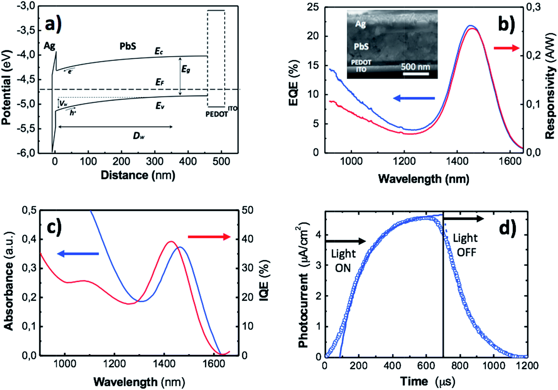 | ||
| Fig. 5 (a) Energy band profile of the Schottky-heterostructure ITO/PEDOT/QD-solid/Ag. (b) External quantum efficiency (blue line) and responsivity (red line) as a function of the light wavelength of the Schottky-heterostructure photodetector. (c) Absorbance (blue line) and photoluminescence (red line) of the photoactive PbS QD-solid film in the wavelength region of interest. (d) Photocurrent transient response measured at 0 V under an incident light at 1550 nm that is chopped at 800 Hz. | ||
From the above presented Schottky-heterostructure photodiode and previous data in literature,24–26 it should be accepted that photogenerated electron–hole pairs in the QD-solid layer will be efficiently separated and collected in Ag (electrons) and ITO (holes) electrodes giving rise to a noticeable photocurrent. In fact, we measured photocurrents in the order of several tens of nanoamperes under 100 nW exposure to light around 1500 nm, and 10–20 mA cm−2 (with VOC ≈ 0.1–0.3 V) under AM1.5 conditions for most of our photodevices (Fig. S8†). On the negative side, mid-bandgap states attributed to lead sulphites species (PbSO3), acting as deep traps for electrons in the p-semiconductor, would influence the barrier height of the Schottky contact and the time response of the device.53,54 On the positive side, the ligand exchange from OAm to MPA would reduce the interspacing between individual QDs and lead to an enhancement of the carrier mobility and lifetime in the QD-solid film,27 due to the electronic coupling between quantum dots that gives rise to Bloch transport of carriers.55
Responsivity (R) curves of the photodiodes were performed to quantify the electrical signal output given by the device per optical power input. This figure of merit represents the ratio of the photocurrent to the power of incident light irradiating the active layer of the detector. Associated to the responsivity, the external quantum efficiency (EQE) defines the efficiency with which an incident photon results on the generation of an exciton. The general expression for the EQE is given by:56
 | (1) |
Fig. 5d shows a period (several periods are shown in Fig. S10†) of the square-shape modulated photocurrent under incident light at 1550 (chopper frequency of 800 Hz). After light-on or light-off conditions, the steady state is reached under exponential dependences I0(1 − exp(−t/τ)) or I0exp(−t/τ), respectively, with a time constant τ ≈ 135 μs after fitting (continuous lines in Fig. 5d) to the experimental curve (data symbols). This temporal response is comparable to similar devices in literature25,58 and it mainly corresponds to carriers photogenerated in the depletion zone of the PbS QD-solid drifting to the metal contact active region, with a minor contribution of carrier diffusion generated at the quasi-neutral region of this layer, because our Schottky-heterostructure device is near fully depleted, as shown below.
The junction electrostatic and conduction characteristics under dark conditions are investigated from capacitance–voltage (C–V) (Fig. 6a) and intensity–voltage (I–V) (Fig. 6b) measurements. From C–V measurements we can estimate the acceptor concentration Na, the built in potential Vbi and the width of the depletion region W, provided the well-known relation for the depletion region formed in the semiconductor (abrupt doping approximation):52
 | (2) |
 | (3) |
 | ||
| Fig. 6 (a) C–V characteristics of the device recorded at a frequency of 8 kHz. (b) I–V characteristics of the device in dark conditions and under illumination with 2 μW at 1550 nm. Continuous curves stand for the best fit to an ideal Schottky diode formula. | ||
The C−2(V) data (open symbols in Fig. 6a) were measured at a frequency of 8 kHz, just in the region where C(ω) is approximately constant (Fig. S11†). It exhibits a linear behaviour around 0 V whose fitting through eqn (2) (continuous line in Fig. 6a) yields a built-in potential Vbi ≈ 0.16 V, an acceptor concentration Na ≈ 1.9 × 1015 cm−3 and a depletion zone width w ≈ 374 nm (eqn (3)). The latter value, as compared to the thickness of the PbS QD film (≈450 nm) indicates that the active layer is mostly depleted. By using this acceptor concentration and the independently measured resistivity in doctor blading films, ρ ≈ 105 Ω cm, a mobility of 0.033 cm2 V−1 s−1 is deduced, which is consistent with values reported in literature.60
The I–V characteristic of our device under dark conditions (red open symbols in Fig. 6b) yields a dark current of only 35 nA (3.5 μA cm−2) at V = −0.05 V, whereas exhibits a photoresponse as high as 286 nA at −0.05 V under monochromatic light exposition of 2 μW at λ = 1550 nm (blue open symbols in Fig. 6b). That means a photocurrent over dark current ratio of around a factor ten. This demonstrates the high sensitivity of our photodetector. The I–V curves were fitted (continuous lines in Fig. 6b) using the ideal diode equation (Iph = 0 under dark conditions):
 | (4) |
The last figures of merit measured in our QD solid-based photodiodes are the noise equivalent power (NEP) and detectivity (D*). The NEP is defined as the level of incident light power that generates a photocurrent equal to the noise current, which is measured to be around 2 pW. The NEP value has been graphically extrapolated to the noise level baseline from the linear response of the measured photocurrent at the peak responsivity wavelength as a function of the incident power (Fig. S12†). The NEP normalized to the electrical bandwidth and to the photosensitive area of the photodetector is the detectivity, which results D* ≈ 1011 jones, comparable to the most efficient photodevices reported in literature.25,50
Conclusions
In summary, we have demonstrated the feasibility of doctor blading to produce close-packed QD solids from a solution-processable PbS QD ink for IR photodetection. This approach provides fast and highly efficient method for large-area deposition of colloidal QD inks in a single or several deposition steps. The use of colloidal QDs as building blocks for the construction of QD-solids requires QDs with high uniformity in composition, size, shape, and surface passivation. Based on that, we produced highly monodispersed OAm-capped PbS QDs that exhibit a well-defined absorption peak at ≈1500 nm with an average particle size of 6.7 nm and a relative size dispersion of 8.5%. Analysis of the crystal structure by XRD and GIXD confirms that the PbS QDs correspond to the PbS bulk with rock salt crystal structure and the complete removal of unreacted PbCl2 after the synthesis. The PbS QD nanoink was formulated using octane as a solvent to achieve the appropriate rheological properties for the doctor blading technology. The original OAm molecules present on the PbS QD surface as well as the drying characteristics of octane lead to an optimal self-organization of QDs into a close-packed BCC superlattice once the nanoink is deposited onto a substrate, which is maintained after MPA ligand exchange, as corroborated by low angle XRD patterns.The solid-state ligand exchange, which is accomplished by replacing the original long OAm molecules by MPA, is confirmed by FTIR, TGA and XPS. As a result, the electrical resistivity of the QD solid after the ligand exchange is reduced around five orders of magnitude (ρ ≈ 105 ohm cm). Further XPS analysis of the PbS QD solids in air before and after the ligand exchange highlights that the principal oxidation product PbSO3 is extremely reduced for ligand exchange times of 60 s. Moreover, we observed the formation of an oxidized shell on the PbS core, which in fact does not affect the structural quality of the bulk-like PbS core and effectively passivates the QD surface. Additionally, we found that the use of Cl− anions in the synthesis induces an additional Cl-based passivation layer that provides a higher stability of the QD-solid upon long-term exposure to air. Moreover, SEM characterization of the resulting solid shows that doctor blading allows the generation of crack-free and homogeneous films. This is of special importance for the development of high-performance QD devices.
Finally, we have developed and characterized a photodetector at telecom wavelengths based on the solution-processed QD solid by doctor blading. Using a simple Schottky-based architecture, the photodiode reached at 1500 nm a R ≈ 0.26 A W−1, D* ≈ 1011 jones and a time response of about 135 μs. These results demonstrate that solids processed from PbS QD nanoinks by doctor blading might pave the way to a cost-effective roll-to-roll compatible technology for the development of advanced multispectral photodetectors and solar cells.
Acknowledgements
This work was supported through the EU-FP7 NAVOLCHI project under grant No. 288869, the Spanish MINECO and Generalitat Valenciana under Grants No. TEC2014-53727-C2-1-R and PROMETEOII/2014/059, respectively. We are grateful to the Electronic Microscopy team at Central Support Service in Experimental Research (SCSIE, University of Valencia, Spain) for their kind and constant support.Notes and references
- J. M. Luther, M. Law, M. C. Beard, Q. Song, M. O. Reese, R. J. Ellingson and A. J. Nozik, Schottky Solar Cells Based on Colloidal Nanocrystal Films, Nano Lett., 2008, 8, 3488–3492 CrossRef CAS PubMed.
- R. Debnath, J. Tang, D. A. Barkhouse, X. Wang, A. G. Pattantyus-Abraham, L. Brzozowski, L. Levina and E. H. Sargent, Ambient-Processed Colloidal Quantum Dot Solar Cells via Individual Pre-Encapsulation of Nanoparticles, J. Am. Chem. Soc., 2010, 132, 5952 CrossRef CAS PubMed.
- A. G. Pattantyus-Abraham, I. J. Kramer, A. R. Barkhouse, X. Wang, G. Konstantatos, R. Debnath, L. Levina, I. Raabe, M. K. Nazeeruddin, M. Grätzel and E. H. Sargent, Depleted-heterojunction colloidal quantum dot solar cells, ACS Nano, 2010, 4, 3374 CrossRef CAS PubMed.
- D. Zhitomirsky, M. Furukawa, J. Tang, P. Stadler, S. Hoogland, O. Voznyy, H. Liu and E. H. Sargent, N-Type Colloidal-Quantum-Dot Solids for Photovoltaics, Adv. Mater., 2012, 24, 6181–6185 CrossRef CAS PubMed.
- A. H. Khan, U. Thupakula, A. Dalui, S. Maji, A. Debangshi and S. Acharya, Evolution of Long Range Bandgap Tunable Lead Sulfide Nanocrystals with Photovoltaic Properties, J. Phys. Chem. C, 2013, 117(15), 7934–7939 CAS.
- K.-S. Cho, E. K. Lee, W.-J. Joo, E. Jang, T.-H. Kim, S. J. Lee, S.-J. Kwon, J. Y. Han, B.-K. Kim, B. L. Choi and J. M. Kim, High-performance crosslinked colloidal quantum-dot light-emitting diodes, Nat. Photonics, 2009, 3, 341 CrossRef CAS.
- Y. Shirasaki, G. J. Supran, M. G. Bawendi and V. Bulovic, Emergence of colloidal quantum-dot light-emitting technologies, Nat. Photonics, 2012, 7, 13 CrossRef.
- B. S. Mashford, M. Stevenson, Z. Popovic, C. Hamilton, Z. Zhou, C. Breen, J. Steckel, V. Bulovic, M. Bawendi, S. Coe-Sullivan and P. T. Kazlas, High-efficiency quantum-dot light-emitting devices with enhanced charge injection, Nat. Photonics, 2013, 7, 407 CrossRef CAS.
- K. Qiao, H. Deng, X. Yang, D. Dong, M. Li, L. Hu, H. Liu, H. Song and J. Tang, Spectra-selective PbS quantum dot infrared photodetectors, Nanoscale, 2016, 8, 7137–7143 RSC.
- G. Konstantatos, I. Howard, A. Fischer, S. Hoogland, J. Clifford, E. Klem, L. Levina and E. H. Sargent, Ultrasensitive solution-cast quantum dot photodetectors, Nature, 2006, 442, 180 CrossRef CAS PubMed.
- G. Konstantatos and E. H. Sargent, Nanostructured materials for photon detection, Nat. Nanotechnol., 2010, 5, 391 CrossRef CAS PubMed.
- J.-S. Lee, M. V. Kovalenko, J. Huang, D. S. Chung and D. V. Talapin, Band-like transport, high electron mobility and high photoconductivity in all-inorganic nanocrystal arrays, Nat. Nanotechnol., 2011, 6, 348 CrossRef CAS PubMed.
- S. Keuleyan, E. Lhuillier, V. Brajuskovic and P. Guyot-Sionnest, Mid-infrared HgTe colloidal quantum dot photodetectors, Nat. Photonics, 2011, 5, 489 CrossRef CAS.
- G. Konstantatos, M. Badioli, L. Gaudreau, J. Osmond, M. Bernechea, F. P. G. de Arquer, F. Gatti and F. H. L. Koppens, Hybrid graphene-quantum dot phototransistors with ultrahigh gain, Nat. Nanotechnol., 2012, 7, 363 CrossRef CAS PubMed.
- F. Pelayo García de Arquer, T. Lasanta, M. Bernechea and G. Konstantatos, Tailoring the Electronic Properties of Colloidal Quantum Dots in Metal–Semiconductor Nanocomposites for High Performance Photodetectors, Small, 2015, 11(22), 2636–2641 CrossRef.
- D. V. Talapin and C. B. Murray, PbSe Nanocrystal solids for n- and p-channel thin film field-effect transistors, Science, 2005, 310(5745), 86–89 CrossRef CAS PubMed.
- M. I. Bodnarchuk, M. V. Kovalenko, S. Pichler, G. Fritz-Popovski, G. Hesser and W. Heiss, Large-Area Ordered Superlattices from Magnetic Wüstite/Cobalt Ferrite Core/Shell Nanocrystals by Doctor Blade Casting, ACS Nano, 2010, 4(1), 423–431 CrossRef CAS PubMed.
- C. R. Kagan and C. B. Murray, Charge transport in strongly coupled quantum dot solids, Nat. Nanotechnol., 2015, 10, 1013–1026 CrossRef CAS PubMed.
- C. B. Murray, C. R. Kagan and M. G. Bawendi, Synthesis and characterization of monodisperse nanocrystals and close-packed nanocrystal assemblies, Annu. Rev. Mater. Sci., 2000, 30, 545–610 CrossRef CAS.
- K. Lambert, L. Wittebrood, I. Moreels, D. Deresmes, B. Grandidier and Z. J. Hens, Langmuir-Blodgett monolayers of InP quantum dots with short chain ligands, J. Colloid Interface Sci., 2006, 300, 597–602 CrossRef CAS PubMed.
- S. Coe-Sullivan, J. S. Steckel, W. K. Woo, M. G. Bawendi and V. Bulovic, Large-Area Ordered Quantum-Dot Monolayers via Phase Separation During Spin-Casting, Adv. Funct. Mater., 2005, 15, 1117–1124 CrossRef CAS.
- Z. Ning, H. Dong, Q. Zhang, O. Voznyy and E. H. Sargent, Solar Cells Based on Inks of n-Type Colloidal Quantum Dots, ACS Nano, 2014, 8(10), 10321–10327 CrossRef CAS PubMed.
- R. Søndergaard, M. Hösel, D. Angmo, T. T. Larsen-Olsen and F. C. Krebs, Roll-to-roll fabrication of polymer solar cells, Mater. Today, 2012, 15, 36–49 CrossRef.
- P. Schilinsky, C. Waldauf and C. J. Brabec, Performance analysis of printed organic solar cells, Adv. Funct. Mater., 2006, 16, 1669–1672 CrossRef CAS.
- Y.-H. Chang, S.-R. Tseng, C.-Y. Chen, H.-F. Meng, E.-C. Chen, S.-F. Horng and C.-S. Hsu, Polymer solar cell by blade coating, Org. Electron., 2009, 10, 741–746 CrossRef CAS.
- D. V. Talapin, J.-S. Lee, M. V. Kovalenko and E. V. Shevchenko, Prospects of Colloidal Nanocrystals for Electronic and Optoelectronic Applications, Chem. Rev., 2010, 110(1), 389–458 CrossRef CAS PubMed.
- G. Konstantatos and E. H. Sargent, Solution-processed quantum dot photodetectors, Proc. IEEE, 2009, 97, 1666–1683 CrossRef CAS.
- J. P. Clifford, G. Konstantatos, K. W. Johnston, S. Hoogland, L. Levina and H. Sargent, Fast, sensitive and spectrally tuneable colloidal quantum dot photodetectors, Nat. Nanotechnol., 2009, 4, 40–44 CrossRef CAS PubMed.
- B. N. Pal, I. Robel, A. Mohite, R. Laocharoensuk, D. J. Werder and V. I. Klimov, High-sensitivity p–n junction photodiodes based on PbS nanocrystal quantum dots, Adv. Funct. Mater., 2012, 22, 1741–1748 CrossRef CAS.
- K. S. Jeong, J. Tang, H. Liu, J. Kim, A. W. Schaefer, K. Kemp, L. Levina, X. Wang, S. Hoogland, R. Debnath, L. Brzozowski, E. H. Sargent and B. John, Enhanced Mobility-Lifetime Products in PbS Colloidal Quantum Dot Photovoltaics, ACS Nano, 2012, 6(1), 89–99 CrossRef CAS PubMed.
- L. Cademartiri, J. Bertolotti, R. Sapienza, D. S. Wiersma, G. von Freymann and G. A. Ozin, Multigram Scale, Solventless, and Diffusion-Controlled Route to Highly Monodisperse PbS Nanocrystals, J. Phys. Chem. B, 2006, 110, 671–673 CrossRef CAS PubMed.
- I. Moreels, K. Lambert, D. Smeets, D. De Muynck, T. Nollet, J. C. Martins, F. Vanhaecke, A. Vantomme, C. Delerue, G. Allan and Z. Hens, Size-Dependent Optical Properties of Colloidal PbS Quantum Dots, ACS Nano, 2009, 3, 3023–3030 CrossRef CAS PubMed.
- D. Zhang, J. Song, J. Zhang, Y. Wang, S. Zhang and X. Miao, A facile and rapid synthesis of lead sulfide colloidal quantum dots using in situ generated H2S as the sulfur source, CrystEngComm, 2013, 15, 2532–2536 RSC.
- R. Abargues, P. J. Rodriguez-Canto, S. Albert, I. Suarezb and P. Martínez-Pastor, Plasmonic optical sensors printed from Ag–PVA nanoinks, J. Mater. Chem. C, 2014, 2, 908–915 RSC.
- B. Derby, Inkjet Printing of Functional and Structural Materials: Fluid Property Requirements, Feature Stability, and Resolution, Annu. Rev. Mater. Res., 2010, 40, 395–414 CrossRef CAS.
- L. Chen and E. Bonaccurso, Effects of surface wettability and liquid viscosity on the dynamic wetting of individual drops, Phys. Rev. E: Stat., Nonlinear, Soft Matter Phys., 2014, 90, 022401 CrossRef PubMed.
- C. Kim, M. Nogi, K. Suganuma and Y. Yamato, Inkjet-Printed Lines with Well-Defined Morphologies and Low Electrical Resistance on Repellent Pore-Structured Polyimide Films, ACS Appl. Mater. Interfaces, 2012, 4, 2168–2173 CAS.
- Y. Diao, L. Shaw, Z. Bao and S. C. B. Mannsfeld, Morphology control strategies for solution-processed organic semiconductor thin films, Energy Environ. Sci., 2014, 7, 2145–2159 CAS.
- C. B. Murray, S. Sun, W. Gaschler, H. Doyle, T. A. Betley and C. R. Kagan, Colloidal synthesis of nanocrystals and nanocrystal superlattices, IBM J. Res. Dev., 2001, 45, 47–56 CrossRef CAS.
- D. V. Talapin, J.-S. Lee, M. V. Kovalenko and E. V. Shevchenko, Prospects of colloidal nanocrystals for electronic and optoelectronic applications, Chem. Rev., 2010, 110, 389–458 CrossRef CAS PubMed.
- D. V. Talapin and C. B. Murray, PbSe nanocrystal solids for n- and p-channel thin film field-effect transistors, Science, 2005, 310, 86–89 CrossRef CAS PubMed.
- M. V. Kovalenko, M. Scheele and D. V. Talapin, Colloidal nanocrystals with molecular metal chalcogenide surface ligands, Science, 2009, 324, 1417–1420 CrossRef CAS PubMed.
- D. N. Dirin, S. Dreyfuss, M. I. Bodnarchuk, G. Nedelcu, P. Papagiorgis, G. Itskos and M. V. Kovalenko, Lead halide perovskites and other metal halide complexes as inorganic capping ligands for colloidal nanocrystals, J. Am. Chem. Soc., 2014, 136, 6550–6553 CrossRef CAS PubMed.
- A. Nag, M. V. Kovalenko, J.-S. Lee, W. Liu, B. Spokoyny and D. V. Talapin, Metal-free inorganic ligands for colloidal nanocrystals: S2−, HS−, Se2−, HSe−, Te2−, HTe−, TeS32−, OH−, and NH2− as surface ligands, J. Am. Chem. Soc., 2011, 133, 10612–10620 CrossRef CAS PubMed.
- Z. Ning, Y. Ren, S. Hoogland, O. Voznyy, L. Levina, P. Stadler, X. Lan, D. Zhitomirsky and E. H. Sargent, All-inorganic colloidal quantum dot photovoltaics employing solution-phase halide passivation, Adv. Mater., 2012, 24, 6295–6299 CrossRef CAS PubMed.
- A. T. Fafarman, W.-k. Koh, B. T. Diroll, D. K. Kim, D.-K. Ko, S. J. Oh, X. Ye, V. Doan-Nguyen, M. R. Crump, D. C. Reifsnyder, C. B. Murray and C. R. Kagan, Thiocyanate capped nanocrystal colloids: a vibrational reporter of surface chemistry and a solution-based route to enhanced coupling in nanocrystal solids, J. Am. Chem. Soc., 2011, 133, 15753–15761 CrossRef CAS PubMed.
- V. Malgras, A. Nattestad, Y. Yamauchi, S. Xue Dou and J. Ho. Kim, The effect of surface passivation on the structure of sulphur-rich PbS colloidal quantum dots for photovoltaic application, Nanoscale, 2015, 7, 5706 RSC.
- N. Zhao, T. P. Osedach, L.-Y. Chang, S. M. Geyer, D. Wanger, M. T. Binda, A. C. Arango, M. G. Bawendi and V. Bulovic, ACS Nano, 2010, 4, 3743–3752 CrossRef CAS PubMed.
- E. J. D. Klem, H. Shukla, S. Hinds, D. D. MacNeil, L. Levina and E. H. Sargent, Impact of dithiol treatment and air annealing on the conductivity, mobility, and hole density in PbS colloidal quantum dot solids, Appl. Phys. Lett., 2008, 92, 212105 CrossRef.
- D. Zherebetskyy, M. Scheele, Y. Zhang, N. Bronstein, C. Thompson, D. Britt, M. Salmeron, P. Alivisatos and L.-W. Wang, Hydroxylation of the surface of PbS nanocrystals passivated with oleic acid, Science, 2014, 344, 1380 CrossRef CAS PubMed.
- W. Ki Bae, J. Joo, L. A. Padilha, J. Won, D. C. Lee, Q. Lin, W.-k. Koh, H. Luo, V. I. Klimov and J. M. Pietryga, Highly Effective Surface Passivation of PbSe Quantum Dots through Reaction with Molecular Chlorine, J. Am. Chem. Soc., 2012, 134(49), 20160–20168 CrossRef PubMed.
- J. P. Clifford, K. W. Johnston, L. Levina and E. H. Sargent, Schottky barriers to colloidal quantum dot films, Appl. Phys. Lett., 2007, 91, 253117 CrossRef.
- S. Espevik, C. Wu and R. H. Bube, The PbS Si heterojunction III: optical properties, J. Appl. Phys., 1971, 42(3513), 1971 Search PubMed.
- G. Konstantatos and E. H. Sargent, Solution-Processed Quantum Dot Photodetectors, Proc. IEEE, 2009, 97(10), 1666–1683 CrossRef CAS.
- D. Zhitomirsky, O. Voznyy, S. Hoogland and E. H. Sargent, Measuring charge carrier diffusion in coupled colloidal quantum dot solids, ACS Nano, 2013, 7, 5282–5290 CrossRef CAS PubMed.
- S. M. Sze and K. K. Ng, Physics of Semiconductor Devices, John Wiley & Sons, 3rd edn, 2007, ch. 13 Search PubMed.
- E. Heves and Y. Gurbuz, Highly Responsive, Solution-Based Al/PbS and Au–Ti/PbS Schottky Photodiodes for SWIR Detection, IEEE Sens. J., 2014, 14(3), 816–820 CrossRef CAS.
- T. Rauch, M. Böber, S. F. Tedde, J. Fürst, M. V. Kovalenko, G. Hesser, U. Lemmer, W. Heiss and O. Hayden, Near-infrared imaging with quantum-dot-sensitized organic photodiodes, Nat. Photonics, 2009, 3, 332–336 CrossRef CAS.
- I. Moreels, D. Kruschke, P. Glas and J. W. Tomm, The dielectric function of PbS quantum dots in a glass matrix, Opt. Mater. Express, 2012, 2(5), 496–500 CrossRef CAS.
- D. M. Balazs, M. I. Nugraha, S. Z. Bisri, M. Sytnyk, W. Heiss and M. A. Loi, Appl. Phys. Lett., 2014, 104, 112104 CrossRef.
Footnote |
| † Electronic supplementary information (ESI) available. See DOI: 10.1039/c6ra14782h |
| This journal is © The Royal Society of Chemistry 2016 |