
 Open Access Article
 This Open Access Article is licensed under a
 Creative Commons Attribution 3.0 Unported Licence
High-efficiency crystalline silicon solar cells: status and perspectives
Corsin
Battaglia
*a,
Andres
Cuevas
b and
Stefaan
De Wolf
c
aEmpa, Swiss Federal Laboratories for Materials Science and Technology, Laboratory Materials for Energy Conversion, 8600 Dübendorf, Switzerland. E-mail: corsin.battaglia@empa.ch
bThe Australian National University, Research School of Engineering, Canberra ACT 0200, Australia
cEcole Polytechnique Fédérale de Lausanne, Photovoltaics and Thin Films Electronics Laboratory, 2000 Neuchâtel, Switzerland
First published on 12th February 2016
Abstract
With a global market share of about 90%, crystalline silicon is by far the most important photovoltaic technology today. This article reviews the dynamic field of crystalline silicon photovoltaics from a device-engineering perspective. First, it discusses key factors responsible for the success of the classic dopant-diffused silicon homojunction solar cell. Next it analyzes two archetypal high-efficiency device architectures – the interdigitated back-contact silicon cell and the silicon heterojunction cell – both of which have demonstrated power conversion efficiencies greater than 25%. Last, it gives an up-to-date summary of promising recent pathways for further efficiency improvements and cost reduction employing novel carrier-selective passivating contact schemes, as well as tandem multi-junction architectures, in particular those that combine silicon absorbers with organic–inorganic perovskite materials.
Broader contextPhotovoltaic solar energy offers humankind a useful instrument to build a globally prosperous, sustainable, and environmentally friendly society. Its recent success as an economically viable source of electricity is founded on a simple optoelectronic device, the crystalline silicon solar cell. The evolution of this device – relatively slow in the past – has accelerated in recent years, posing now new challenges and opening exciting opportunities. This review is both comprehensive and up to date, describing prior, current and emerging technologies for high-efficiency silicon solar cells. It will help the reader understand how crystalline silicon solar cells work, how they are made, and which factors limit their performance. It then describes several approaches to overcome such limitations, and how these approaches are being transferred from research laboratories to the industry. Specific attention is given to two device designs, the interdigitated back contact cell and the silicon heterojunction cell, pointing out their salient features, critical in enabling very high power conversion efficiencies. Despite its proven maturity, silicon solar cell technology continues receiving an influx of important new ideas that promise simpler fabrication and higher performance. A prime example is its combination with other semiconductor materials to build tandem devices for ultra-high efficiencies. |
The year 2014 witnessed the breaking of the historic 25.0% power conversion efficiency record for crystalline silicon solar cells, which was set by the University of New South Wales (UNSW), Australia, in 1999.1,2 Almost simultaneously, Panasonic, Japan,3 and SunPower, USA,4 reported independently certified efficiencies of 25.6% and 25.0%, respectively, both using industrially-sized silicon wafers (see Fig. 1 and Table 1). In parallel, the increased production volumes and associated maturity of the technology have brought the cost of photovoltaic modules down to 0.62 US$/Wp (average price in 2014 according to the International Technology Roadmap for Photovoltaics).5 Solar photovoltaic electricity has already reached grid parity in many countries and locations. While costs associated with cell processing typically account for less than 20% of the total module cost and only about 10% at the system level,5 increasing the power conversion efficiency of the solar cell offers a direct pathway to further reducing the levelized cost of electricity (LCOE).6–8 This review retraces recent advances in silicon solar cell technology towards that goal. The reader may be interested in consulting complementary reviews by Saga9 and Glunz.10 A detailed life cycle assessment including a discussion of indicators such as primary energy demand, energy payback time and greenhouse gas emissions can be found in ref. 11.
 | ||
| Fig. 1 Evolution of the energy conversion efficiencies of silicon photovoltaics according to year of entry in tables of ref. 12. Note the steep efficiency improvement of cells with an area larger than 100 cm2. The step increase in efficiency in 2009 is due to the redefinition of the standard solar spectrum and affects all technologies. | ||
| Device | Area [cm2] | V oc [mV] | J sc [mA cm−2] | FF [%] | Eff. [%] | Certification |
|---|---|---|---|---|---|---|
| Ideal, 110 μm | 761 | 43.3 | 89.3 | 29.4 | Modeled17 | |
| Panasonic IBC HIT | 143.7 (da) | 740 | 41.8 | 82.7 | 25.6 | AIST (2/14)3 |
| SunPower IBC | 153.5 (ta) | 737 | 41.3 | 82.7 | 25.2 | Fraunhofer ISE (10/15)12 |
| Kaneka SHJ | 151.9 (ap) | 738 | 40.8 | 83.5 | 25.1 | Fraunhofer ISE (9/15)370 |
| Fraunhofer ISE TOPCon | 4.0 (da) | 718 | 42.1 | 83.2 | 25.1 | Fraunhofer ISE (8/15)290,371 |
| UNSW PERL (p-type) | 4.0 (da) | 706 | 42.7 | 82.8 | 25.0 | Sandia (3/99)1,12 |
| Panasonic HIT | 101.8 (ta) | 750 | 39.5 | 83.2 | 24.7 | AIST (12/12)218 |
| EPFL MoOx SHJ | 3.9 (ap) | 725 | 38.6 | 80.4 | 22.5 | Fraunhofer ISE (2015)310 |
| imec PERT (n-type) | 238.9 (ta) | 695 | 40.2 | 80.5 | 22.5 | Fraunhofer ISE (2015)160,174 |
| Trina solar mono-Si PERC (p-type) | 243.7 | 680 | 40.5 | 80.3 | 22.1 | Fraunhofer ISE (2015)12,315 |
| Trina solar multi-Si PERC (p-type) | 242.7 (ap) | 667 | 39.8 | 80.0 | 21.3 | Fraunhofer ISE (11/15)12,372 |
Compared to other photovoltaic technologies, silicon solar cells have the advantage of using a photoactive absorber material that is stable, non-toxic, abundant and well understood. Silicon has an energy band gap of 1.12 eV, corresponding to a light absorption cut-off wavelength of about 1160 nm. This band gap is well matched to the solar spectrum, very close to the optimum value for solar-to-electric energy conversion using a single semiconductor optical absorber. Taking only radiative recombination into account (the so-called detailed balance),13 the theoretical conversion efficiency limit for a semi-infinitely thick silicon solar cell is 33.5% at 25 °C.14
Silicon has an indirect energy band gap, i.e. the valence band maximum is not at the same position in momentum space as the conduction band minimum. This has two major consequences. First, it makes radiative recombination fairly inefficient, which implies that, for defect-free material, the photogenerated electrons and holes can exhibit very long lifetimes. In fact, rather than its radiative counterpart, the dominant intrinsic recombination mechanism in silicon is Auger recombination, in which an electron recombines with a hole by transferring their energy difference to a third charge carrier, either a second free electron or hole. This energy is subsequently lost as heat. Consequently, based on an empirical parameterization of experimentally measured radiative and Auger recombination rates,15 the limiting intrinsic efficiency for silicon solar cells has been calculated to be 29.4% – significantly lower than the detailed balance limit (for an optimum thickness of 110 μm and considering Lambertian light trapping,16Fig. 2 and Table 1).17 Secondly, because of its indirect band gap, silicon also has a relatively low light absorption coefficient, particularly near its band gap (for a comparison of absorption coefficients of several photovoltaic materials, see, e.g., ref. 18). Despite this, with simple wafer surface texturing, combined with the use of well-designed antireflection coatings and rear surface mirrors, efficient light absorption, including the infrared part of the solar spectrum, is possible even with relatively thin wafers (∼100–150 μm).17 In practice, carrier recombination in silicon can be affected, or even dominated, by the presence of crystallographic defects or foreign impurities. In recent years, thanks to improved silicon ingot growth processes, defect engineering and contamination control during solar cell fabrication, the bulk electronic quality of crystalline silicon wafers has improved to such a point that further device advances now rely on innovative interface passivation and carrier-selective contact structures.
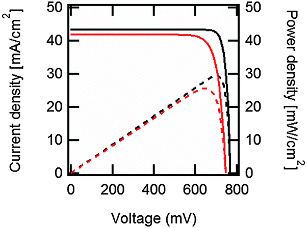 | ||
| Fig. 2 Output current density (continuous black line) and output power density (dashed black line) vs. voltage under one-sun illumination for the ideal, Auger-limited, crystalline silicon solar cell with silicon absorber thickness of 110 μm, open-circuit voltage of 761 mV, short-circuit current density of 43.3 mA cm−2, fill factor of 89.3%, and power conversion efficiency of 29.4%.16 In red are the corresponding curves for the current world-record silicon solar cell from Panasonic, with an open-circuit voltage of 740 mV, a short-circuit current density of 41.8 mA cm−2, a fill factor of 82.7% and a power conversion efficiency of 25.6%.207 These approximate curves were generated using eqn (7) with ideality factors n = 0.675 for the ideal cell, and n = 1, plus a series resistance of 0.61 Ω cm2, for the world-record cell. | ||
The main purpose of interface passivation is to reduce recombination of photogenerated carriers at the silicon surface.19–21 This can be done by chemical passivation – usually by hydrogen – of harmful surface defects,22–25 which are predominantly broken silicon–silicon bonds, called dangling bonds, or by modifying the relative concentration of photogenerated electrons and holes near the surface.26,27 Effective surface passivation is usually achieved by dielectric materials such as silicon oxide,26,28–32 silicon nitride,33–36 silicon carbide37,38 and aluminum oxide.19,39–41 Alternatively, a (disordered) semiconductor such as intrinsic hydrogenated amorphous silicon42,43 can be employed. None of these layers allows carrier extraction per se, as they are either insulating or insufficiently conductive.
To enable efficient carrier extraction to the two external metal terminals, two carrier-selective contact structures are needed, which ideally exhibit efficient transport of only one type of carrier (e.g., electrons) while hindering the transport (that is, blocking) of the other type of carrier (e.g., holes). Since recombination requires the participation of both types of carriers, hindering the transport of one of them contributes to reducing recombination in the contact structure. Nevertheless, to suppress recombination more effectively, it is usually necessary to insert in the structure an interfacial passivating layer. Hence a highly selective contact is one that simultaneously presents a high conductivity for just one of the two carriers, while minimizing recombination. In designing high-efficiency solar cells, one may choose either to cover most of the wafer surface with a passivating dielectric material and extract photogenerated carriers selectively through local openings in this insulator,1 or to deposit carrier-selective materials on the full wafer surface using a suitable interface-passivation strategy. In the latter approach, the two simultaneous requirements of surface passivation and preferential conduction are frequently achieved by using a stack of two or more layers, for example intrinsic and doped hydrogenated amorphous silicon, as in silicon heterojunction solar cell technology.44–46
An important criterion for this decision relies on the optical properties of the required materials for contact formation. Indeed, layers blanket-deposited on the wafer surfaces (either for interface passivation or selective transport) should also maximize light coupling into the silicon absorber by minimizing reflection and parasitic absorption losses. Developing contact layers that satisfy these electronic and optical requirements simultaneously represents a considerable challenge. This paper gives a brief overview of recent research to solve it.
1. Basic operation and performance indicators of the solar cell
To grasp the full challenge of fabricating simple high-efficiency solar cells, it is useful to briefly reflect on their essential performance parameters. For this, we first consider a solar cell in its most fundamental form, consisting of a semiconductor with a given energy band gap and electron- and hole-selective contact regions that guarantee charge-carrier separation.When solar radiation strikes the solar cell, photons with energy greater than the band gap of the semiconductor are absorbed, exciting electrons from the valence band into the conduction band, leaving behind an equally large number of holes in the valence band. Consequently, the total electron and hole concentrations (n and p) under illumination deviate from their thermo-chemical equilibrium values in the dark (n0 and p0, with n0p0 = ni2, where ni is 8.3 × 109 cm−3 at 25 °C for silicon).47 A net electric current eventually results when those negative (electrons) and positive (holes) charge carriers move in opposite directions in the device. In the quasi-neutral regions of the device, the excess carrier densities (Δn = n − n0, and Δp = p − p0) are approximately equal Δn ≈ Δp. In analogy to equilibrium, in which the carrier populations are described by a single Fermi energy EF, the carrier populations in non-equilibrium conditions can be described by means of the electron and hole quasi-Fermi energies EFn and EFp48
 | (1) |
 | (2) |
 | (3) |
Under steady-state illumination, photogenerated charge carriers either flow to an external circuit as electric current or they recombine inside the device. In open-circuit conditions, the concentration of carriers builds up, so that the photogeneration rate is perfectly counterbalanced by the recombination rate. As indicated by eqn (3), such high carrier concentration produces the maximum voltage that can be measured in a solar cell, the open-circuit voltage Voc. For electric current to flow, the solar cell needs to be connected to an external circuit by means of two low-resistance selective contacts – one for the electrons and another for the holes. The current is highest at short circuit (zero voltage), when the concentration of carriers inside the device and, therefore, their recombination rate are relatively low. Note, however, that neither the concentration of carriers nor the difference between the quasi-Fermi energies is zero, even if the terminal voltage is. In a good solar cell, the short-circuit current density Jsc is only slightly lower than the number of photons absorbed in the semiconductor per unit time and area, multiplied by the elementary charge, which can be called the photogenerated current density Jph. The ratio between Jsc and Jph is an indication of the “collection efficiency,” that is, of the ratio of electrons out to photons in. This quantum collection efficiency is usually measured as a function of the wavelength, or energy, of the incident photons. For silicon, with its band gap of 1.12 eV, the highest obtainable Jph value for a 110 μm-thick wafer is 43.3 mA cm−2 under standard test conditions (air mass 1.5 global spectrum, 1000 W m−2, 25 °C) (Table 1).
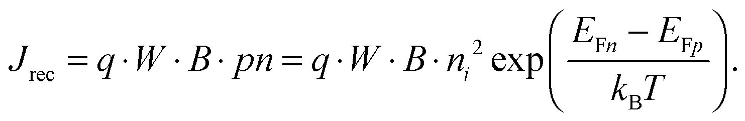
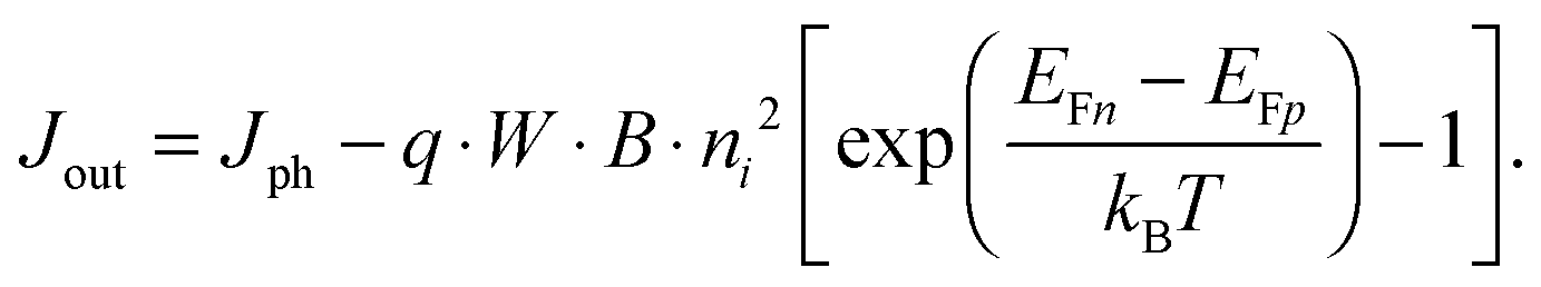
For power generation, the solar cell needs to deliver current and voltage simultaneously, and the total output current density can be written as Jout = Jph + Jeq − Jrec, where we have defined the photogenerated current density Jph as the net cumulative generation in excess of the equilibrium thermal generation, represented by Jeq. The recombination current density Jrec represents all generated carriers that are lost and not collected per unit time and area. Such recombination stems from the higher concentration of electrons and holes required to deliver voltage, compared to short circuit, as shown by eqn (3). Of all loss mechanisms, the most fundamental is radiative band-to-band recombination, which is the inverse process of absorption and is unavoidable. Actually, efficient external luminescence due to radiative recombination is a signature of high-efficiency solar cells,49,50 as it indicates that very few carriers are lost to recombination via defects. Radiative recombination is proportional to the concentrations of the two “reactant species,” that is, to the pn product of the concentrations of holes and electrons.48 The constant of proportionality is called the band-to-band recombination coefficient, which for silicon takes a value of B = 4.73 × 10⁻¹⁵ cm3 s−1 at room temperature.51 Although, as mentioned above, radiative recombination is not dominant in silicon, it is the most fundamental recombination process in any type of photovoltaic absorber and focusing on it helps to elucidate the basic operation principles of solar cells. Using eqn (1) and (2), we can express the total band-to-band recombination current density occurring in a silicon wafer of thickness W as
 | (4) |
| Jeq = q · W · B · p0n0 = q · W · B · ni2. | (5) |
 | (6) |
 | (7) |
Although the above derivation was made for the band-to-band radiative mechanism, other contributing processes to J0 in silicon are Auger and defect-assisted recombination, which are also proportional to the pn product. Indeed, real devices are usually dominated by non-radiative recombination. The Auger recombination mechanism is peculiar, because it involves three carriers, even though its end result is to annihilate one free electron and one free hole. Auger recombination is in principle proportional to the pn product multiplied by the concentration of the majority carriers, p or n, but in practice it deviates slightly from an ideal p2n (or n2p) dependence due to Coulombic interaction between carriers.15,53 Defect-assisted, or Shockley–Read–Hall,54,55 recombination is a two-particle process that can have a complex dependence on the carrier concentrations themselves and on the properties of the defects. Including these additional recombination losses into the solar cell equation requires adapting the J0 prefactor and the ideality factor n, which can become either smaller or greater than one.56 Usually, J0 and n are determined experimentally,57 and their values may reflect a combination of several mechanisms. Low values of J0, implying low recombination, and low values of n are desired for high-efficiency solar cells (see Fig. 2 caption).
Maximum power generation occurs when there is an optimal trade-off between carriers exiting the device, which demands a low concentration of carriers to reduce recombination, and voltage production, which demands a high concentration of carriers. This optimum defines the so-called maximum power point, with associated Jmpp and Vmpp values. The fill factor FF is defined by the ratio (Jmpp·Vmpp)/(Jsc·Voc), and it indicates what fraction of the separate highest current Jsc and voltage Voc can be delivered simultaneously by the solar cell. The maximum value theoretically possible for the fill factor of a silicon solar cell is 89.3%, when considering only intrinsic recombination processes, namely Auger and radiative recombination (Fig. 2). In practice it can be negatively affected by other internal recombination losses and external shunts. The latter present a path for a leakage current to flow directly between the two terminals of the device. The fill factor is further lowered by resistive losses, due to the flow of current through materials with finite conductivity or cross-sectional area, or across interfaces between different materials (for example, the contact resistance between metals and semiconductors). These effects are usually represented in a simplified manner by lumped series and shunt resistance parameters, Rs and Rsh, respectively, which can be incorporated into an expanded form of eqn (7). Resistive losses are usually more severe than shunts, and they can be exacerbated by poor cell design.58 Accurate diagnosis of the Rs parameter, for which various methods exist,59 is essential in high-efficiency solar cell development.60
The delicate balance between the parameters described above determines the power conversion efficiency, η = Voc·Jsc·FF, which is typically measured with a solar radiation simulator under standard test conditions for terrestrial applications (air mass 1.5 global spectrum, 1000 W m−2, 25 °C).61
2. The classic silicon solar cell
2.1. Solar cell structure and performance modelling
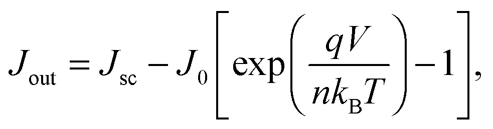
As will be described in subsequent sections, there are several different ways in which electron- and hole-selective contacts can be implemented on a silicon wafer. Classically, they have been formed by introducing a high concentration of dopants near the two surfaces of the wafer. Fig. 3 shows the schematic structure of such a solar cell, based on a p-type crystalline silicon wafer, a front phosphorus diffusion, and a back aluminum-doped region. For the classic dopant-diffused homojunction silicon solar cell, the choice of p-type material stems from both historical and technological reasons. The first applications of silicon solar cells in the 1950s were to power satellites, where p-type cells featured improved space-radiation hardness, compared to their n-type counterparts.62,63 Historically, this n+pp+ solar cell structure has been referred to as BSF (back surface field), even though the equilibrium electric field cannot physically exert a net force on charge carriers.64,65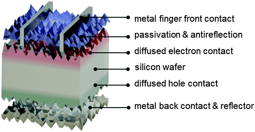 | ||
| Fig. 3 Schematic of the components of a classic dopant-diffused silicon homojunction solar cell. Electrons and holes generated in the textured p-type silicon wafer are extracted via phosphorus-doped (front, red) and aluminum-doped (back, green) regions. The front surface is passivated with hydrogenated amorphous silicon nitride, which acts simultaneously as antireflection coating. Aluminum is employed as the back contact and serves as a dopant source during firing. | ||
The most widespread industrial fabrication method for wafer-based silicon solar cells will be described below. The solar cell performance parameters that can be obtained in practice deviate from their “ideal” values. It is important to identify the most important limitations of the classic silicon solar cell structure, in order to understand the device designs and technology improvements that have already been, or are in the process of being, adopted by the photovoltaic industry. Fig. 4 and 5 present modelling results of the classic n+pp+ structure with the program PC1D,66 using parameters that are representative of many industrial silicon solar cells: a p-type wafer with a dopant density of 1 × 1016 cm−3, thickness of 150 μm, and minority-carrier lifetime of 100 μs; n+ front phosphorus diffusion with a surface concentration of 1 × 1020 cm−3, depth of 0.36 μm, sheet resistance of 100 Ω □−1, and front surface recombination velocity of 104 cm s−1; p+ aluminum-doped region with a surface concentration of 1 × 1019 cm−3, depth of 5 μm, sheet resistance of 40 Ω □−1, and rear surface recombination velocity of 107 cm s−1.
 | ||
| Fig. 4 Energy band diagrams of a classic n+pp+ silicon solar cell (a) in equilibrium and (b) at the maximum power point. Representative values were used to model the curves with the program PC1D66 (p-type wafer doped with 1 × 1016 cm−3 boron atoms, front n+ phosphorus diffusion with a surface concentration of 1 × 1020 cm−3 and depth of 0.36 μm, and back p+ aluminum-doped region with a surface concentration of 1 × 1019 cm−3 and a depth of 5 μm). (c) The electron and hole conductivities at the maximum power point, indicating that the n+ and p+ regions preferentially transport electrons or holes, respectively. | ||
 | ||
| Fig. 5 Analysis of recombination losses of the exemplary n+pp+ silicon solar cell described in Fig. 4. At the maximum power point, the main recombination loss occurs at the rear metal/semiconductor interface, while the p-type absorber region contributes 26% and the front n+ phosphorus diffusion (including its surface) contributes 24%. | ||
Fig. 4a shows the energy band diagram in equilibrium for such a silicon solar cell. The bending of the bands in the vicinity of both diffused regions indicates (i) that the concentrations of electrons and holes vary strongly with position (which can be described as a gradient of their chemical potentials), and (ii) that an electric field (evidenced by the gradient of the bands) is present. These two forces, the gradients of the chemical and electrical potentials, are identical in magnitude and opposite in direction, meaning that there is no net force acting on the carriers and no net movement, as indicated by the constant Fermi energy EF. The energy band diagram in Fig. 4b shows that, at the maximum power point, the Fermi energy splits into two quasi-Fermi energies, as a consequence of the excess concentration of carriers generated by the one-sun illumination. Although indistinguishable in the graph, a very small gradient of the quasi-Fermi energies drives electrons to the left and holes to the right. The reason for such directional flow of the two charge carriers can be seen in Fig. 4c, which shows that the electron conductivity is orders of magnitude higher than the hole conductivity on the left (the n+ region), and the hole conductivity much higher than the electron conductivity on the right (in the p+ region). The predicted conversion efficiency of this solar cell is 21.1% (Voc = 643 mV, Jsc = 39.3 mA cm−2, FF = 83.6%), neglecting any series or shunt resistance effects. A loss analysis at the point of maximum output power (Vmpp = 565 mV, Jmpp = 37.4 mA cm−2), is shown in Fig. 5. Although hypothetical, this example is representative of real devices, and it indicates that output power is limited by recombination at the rear metal contact and in the absorber region, with the front phosphorus diffusion, and its surface also causing significant losses.
2.2. Typical fabrication process
In the photovoltaic industry today, most solar cells are fabricated from boron-doped p-type crystalline silicon wafers (Fig. 3), with typical sizes of 125 × 125 mm2 for monocrystalline silicon (pseudosquare) and 156 × 156 mm2 for multicrystalline silicon (square), and a resistivity of about 1 Ω cm. Monocrystalline silicon wafers are wire-cut from silicon ingots, grown using the Czochralski process, whereas multicrystalline wafers are cut from cast silicon blocks. Wire-cutting traditionally uses slurries,67 but in recent years diamond-coated wires have increasingly been used for this purpose, enabling cutting speeds six to eight times faster, and are expected to become the dominant wafering technology.68,69 The thickness of the cut wafers is typically 180 μm, with a trend towards thinner wafers during the last 15 years.5,70–73 The kerf loss is typically on the order of 100 μm, representing an important cost factor.Silicon solar cell manufacturing typically starts with chemical etching and surface texturing of the wafers.74 Usually, texturing is achieved by immersion of the wafers in a wet chemical bath, yielding identically textured surfaces at the front and back surfaces. The same step also removes several μm of damaged material resulting from the wire sawing. Potassium hydroxide (KOH) etching of (100)-oriented monocrystalline silicon wafers is anisotropic and results in randomly sized square pyramids with (111) faces,75 which reflect and refract the incident light at oblique angles, resulting in excellent antireflection and light-trapping properties.76 Texturing of multicrystalline silicon, which has grains of many different orientations, requires isotropic wet etching, usually based on acidic solutions.77–80 The reflectance of multicrystalline wafers after acidic texturing is higher than that of monocrystalline silicon after alkaline texturing. However, after deposition of an antireflection coating and encapsulation under glass in the module, the total photogeneration in a multicrystalline cell can reach 99% of that in a monocrystalline cell.81 For multicrystalline wafers, various types of submicron texture have been proposed to further improve reflectance.82,83 Very good results have also been reported using plasma texturing.31
After surface texturing (particularly after alkaline etching), the wafers need to be cleaned. Several strategies that usually include at least two steps are possible. First, a chemically oxidizing agent, e.g., an acidic peroxide solution, forms an oxide that “encapsulates” potentially harmful impurities present on the surface. Following rinsing in de-ionized water, the oxide is stripped off in a reducing chemical, usually hydrofluoric acid, which yields relatively inert (111) surfaces with hydrogen termination.84 The wafers are now ready for dopant diffusion, usually phosphorus, for the typical p-type silicon wafer, or boron, if an n-type wafer is used.
Diffusion is usually performed in high-temperature quartz furnaces by exposing the wafers to a gaseous environment containing the phosphorus atoms, typically nitrogen saturated with phosphorus oxychloride (POCl3). A small amount of oxygen is also introduced in the furnace so that a phosphorus–silica glass is grown on the wafer surfaces. It is from this glass that the actual diffusion of the dopant atoms into the silicon wafer takes place. Typical diffusion temperatures range from 760 to 850 °C for phosphorus, and slightly higher for boron. As the doping process is not selective, a diffused region is also formed on the rear and at the edges of the wafer and needs to be subsequently etched off. Typically, the sheet resistance of the resulting n+-type layer is in the 50–100 Ω □−1 range. Following diffusion, the phosphorus–silica glass is etched in hydrofluoric acid; at this point it is possible to also etch a very small amount of silicon to fine-tune the sheet resistance.
The primary purpose of forming a diffused region is charge separation. The n+-type layer at the front surface functions as an electron-selective contact, or electron transport region, by making the concentration of electrons much higher than that of holes, that is, by creating a large asymmetry between the conductivities for electrons and holes (see Fig. 4c). It would seem desirable that the concentration of phosphorus be as high as possible (the maximum electrically active concentration in silicon is about 3 × 1020 cm−3). However, such a high carrier concentration triggers detrimental electronic effects,85–87 including band gap narrowing and three-particle Auger recombination, which draws holes into the n+ region and thus reduces the selectivity of the contact, that is, its ability to “block” holes. Excess phosphorus can form precipitates, which may cause additional recombination. Auger, and possibly Shockley–Read–Hall, recombination not only limits the achievable voltage, but also reduces the blue response of the solar cell.86 A second function of the n+ layer is to connect the wafer absorber region to a metal electrode. To achieve a sufficiently low contact resistance between the metal and the semiconductor, a high concentration of phosphorus (typically in the 1 × 1020 cm−3 range) is required to promote quantum-mechanical tunneling across a thin potential barrier that arises as a consequence of the different work functions (electrochemical potentials) of the two materials.88 The prevalent approach in industry is to implement a phosphorus diffusion with a high surface concentration to achieve a low contact resistivity,89 while being very shallow to reduce absorption of ultraviolet and blue light and thus maintain a reasonable blue response; typically, the junction depth is between 0.2 and 0.3 μm below the surface. Such diffusion is susceptible to surface recombination losses, and a passivating insulator is usually deposited to suppress such losses.34 Since the metal contact is restricted to about 5% of the front surface, the diffused region must also provide lateral transport of the collected electrons towards the metal fingers that form the front electrode. The trade-off between the competing factors of carrier separation, bulk and surface recombination and lateral current transport makes the optimization of the front dopant diffusion quite complex, as discussed below in greater detail.
Phosphorus diffusion offers the additional advantage of impurity gettering. Briefly, gettering is the process where transition metals like iron, nickel, chromium, etc.90–92 diffuse from the bulk of the wafer towards the phosphorus diffusion.93,94 Once they are in the highly doped n+ surface region, these impurities are no longer harmful to device operation.95 This means that relatively impure, and thus cheaper, wafers can be used, making the complete cell process more cost effective. Phosphorus gettering has undoubtedly enabled the development of multicrystalline silicon solar cells.
Wafers are subsequently covered by an antireflection coating with a high transparency across the visible and infrared regions of the spectrum.96,97 The refractive index of the coating should be the geometric mean of the refractive indices n of glass (n ≈ 1.5) and silicon (n ≈ 4 in the visible), while its optical thickness dictates the wavelength at which minimum reflection occurs, which for terrestrial application is preferentially set around 600 nm.98,99 Hydrogenated amorphous silicon nitride (thickness ≈ 75 nm, n ≈ 2 in the visible), often just called silicon nitride, deposited by plasma-enhanced chemical vapor deposition at intermediate temperatures (about 400 °C) has been very successful for this purpose.100 Like the phosphorus diffusion, this layer has multiple functions. In addition to its antireflective properties, silicon nitride provides very efficient passivation of the phosphorus-doped surface.34 Combined with a moderately doped n+ diffusion (sheet resistance of about 100 Ω □−1), it can result in low recombination current densities of 100 fA cm−2 or less.19 Such excellent passivation is due mainly to hydrogen termination of silicon dangling bonds at the surface.35 In addition, silicon nitride layers contain a high positive fixed charge density (∼1012 elementary charges per cm2),101,102 which further increases the concentration of electrons and decreases that of holes at the surface, resulting in a reduced statistical probability of recombination, according to the Shockley–Read–Hall model. Hydrogenated silicon nitride has an added beneficial effect for multicrystalline silicon wafers, as the hydrogen contained in these films is released into the silicon wafer during the so-called contact firing step at the end of the cell process.77,103 The beneficial effect of hydrogenation on defective silicon was already established in 1980.104 Firing of the front metal contact through the silicon nitride layers has proven to passivate defects in multicrystalline silicon wafers very effectively, and it complements the prior POCl3 gettering step.105,106 In the modelling presented in Fig. 5 a minority-carrier lifetime of 100 μs was assumed, but much longer carrier lifetimes have been achieved, thanks to the combined effects of gettering, hydrogenation, and improved ingot growth technologies.
The front side is finalized by screen printing over the antireflection coating an array of silver finger gridlines (width 50–100 μm) usually connected by several busbars and, on top of the busbars, copper–tin stripes (width 1–2 mm). The screen printing paste contains a binder material (glass frit) that dissolves the metal powder, reacts with the silicon nitride and wets the silicon surface during high-temperature firing. During cooling, silver particles precipitate and adhere to the surface of the silicon wafer.107–110 It is critical to minimize shading, by reducing the width of the grid lines, in order to maximize the short-circuit current, but there is a trade-off between shading and resistive losses that needs to be optimized. Minimization of the metal/semiconductor contact fraction is critical to achieve a high voltage (see Fig. 5), but the contact fraction needs to be balanced against an increased contact resistance loss.
During the same firing-through step, the back contact is also formed. Usually a screen-printed aluminum paste is applied over the full back surface of the wafer.107,111–113 During firing, the aluminum forms a eutectic melt with silicon, consuming a similar amount (about 5–20 μm) of silicon. This fully melts and compensates (over-dopes with aluminum) the parasitic n-type region formed at the rear during phosphorus diffusion. During cooldown, a heavily aluminum-doped p-type epitaxial silicon layer forms near the rear surface of the wafer. In addition, this p-type region acts as a hole-selective contact to the p-type silicon absorber. Similar to what was observed above about the n+ region, it would be desirable to implement a very high concentration of aluminum dopant atoms (hence of holes), but the solubility of aluminum in silicon is limited to about 1 × 1019 cm−3. The selectivity of this contact region in terms of blocking electrons is limited by heavy-doping effects such as band gap narrowing114,115 and Auger recombination,116 whereas impurity and carrier–carrier scattering, which limit the minority-carrier mobility, are beneficial in this instance. The eutectic mix that remains on the wafer makes it impossible to apply dielectric coatings to passivate the wafer surface, unless it is etched off. This can lead to high recombination losses, as shown in Fig. 5. To keep minority electrons from reaching the rear metal/silicon interface, a thick p+ layer is used, so that the total conductance (conductivity divided by distance) for the electrons is low. Optimized aluminum-doped regions can reach a recombination current parameter J0 of about 500 fA cm−2,117 but a value of 1000 fA cm−2 is more typical. The latter can be expressed in terms of an effective surface recombination velocity of about 1000 cm s−1 (note that, for a given aluminum-doped region, the surface recombination velocity scales inversely with the dopant density of the wafer, in low injection). The aluminum also acts as a back reflector, albeit a poor one118,119 (that is made even worse by the alloying process), reflecting back into the silicon absorber a fraction of the infrared light that has not been fully absorbed during the previous passage through the silicon wafer.120 Silver-paste strips are usually printed on the rear to enable soldering to the copper interconnects, which “string” the front grid of one cell to the back contact of the neighboring cell in a module. Finally, the parasitic phosphorus diffusion present at the edges is removed by laser scribing around the perimeter of the wafer.
Next, each solar cell is individually measured and sorted according to efficiency and current. The latter is of extreme importance, as cells are connected in series to form strings, which requires that each individual cell contribute an identical current. The module is finished by encapsulating the solar cell strings between a front glass plate and a polyethylene terephthalate (PET) or tedlar/PET/polyamide (TPA) back sheet by means of a lamination process that includes melting of an ethylene vinyl acetate (EVA) sheet.
Industrial silicon solar cells fabricated with the process scheme described here, or variations of it, typically deliver efficiencies of up to 19.5% for monocrystalline and up to 17.8% for multicrystalline substrates.121 Advances in module technologies, including the use of antireflection coatings on the outer glass, result in cell-to-module power ratios close to 100%.5 Nevertheless, the frame, interconnection and other losses cause module efficiencies to be typically 1.5–2% lower than the cell efficiencies.
The great simplicity and robustness of multicrystalline silicon technology explains its current dominance in the photovoltaics market, with a share of about 56%.122 However, over the past years, the price of silicon has dropped significantly, while its electronic quality has improved.6 As a consequence, monocrystalline silicon has become increasingly attractive for solar cell fabrication, with a current market share of about 35%. To fully exploit the benefits of such higher quality material, more sophisticated device designs and fabrication processes are needed. To guarantee overall lower $/Watt values, compared to multicrystalline technology, such processes should remain cost effective and deliver high efficiency. Several factors explain the drive towards higher efficiency silicon solar cells. High-efficiency solar modules require less mounting hardware and space and result in a lower balance-of-system cost. Such modules also yield higher energy densities, which may be important for applications where space is at a premium. Higher efficiency solar cells also usually perform better at higher ambient temperatures and reduced illumination levels, compared to their lower efficiency counterparts. To further increase the energy yield, high-efficiency modules can be combined with solar tracking systems.123
While today's state-of-the-art R&D silicon solar cells can deliver efficiencies above 25%, the performance of industrial cells remains constrained by economic factors. Many of the features enabling high efficiency cause a significant rise in processing or equipment costs. However, identifying and understanding the limitations of the traditional process scheme enables the development of innovative concepts that might lead to higher efficiencies at lower cost. In the following we first discuss briefly how the standard dopant diffusion technology can be “upgraded” towards higher efficiencies. Next, we discuss two archetypal high-efficiency cell architectures, namely interdigitated-back-contact and silicon heterojunction solar cells. Finally, we discuss recent trends combining high voltage and current, as well as simple processing, by using alternative self-passivating and dopant-free contacting schemes.
3. Increasing the efficiency of silicon solar cells
3.1. Selective front diffusions
A good strategy to improve the performance of industrial silicon solar cells is to address step-by-step the individual limitations of the classic technology. A first modification is the decoupling of the requirements of the front diffused region in terms of carrier collection and, on the other hand, high voltage and good contact. As described in Section 2.2., this region is usually very thin, moderately doped and surface passivated, to ensure a high quantum collection efficiency. On the other hand, a high dopant concentration is usually needed to guarantee good contact formation by screen printing. In addition, a deep and highly doped diffusion is desirable to reduce recombination in the fraction of the front surface contacted by the metal grid. Selective diffusion (also called selective-emitter) technology resolves this trade-off by featuring a lowly doped region between the metal fingers, while creating a high doping level just below the fingers. Several approaches have been proposed for the fabrication of such structures, including selective diffusion, ion implantation and laser doping processes.124–1293.2. Localized back contacts and dielectric back surface passivation
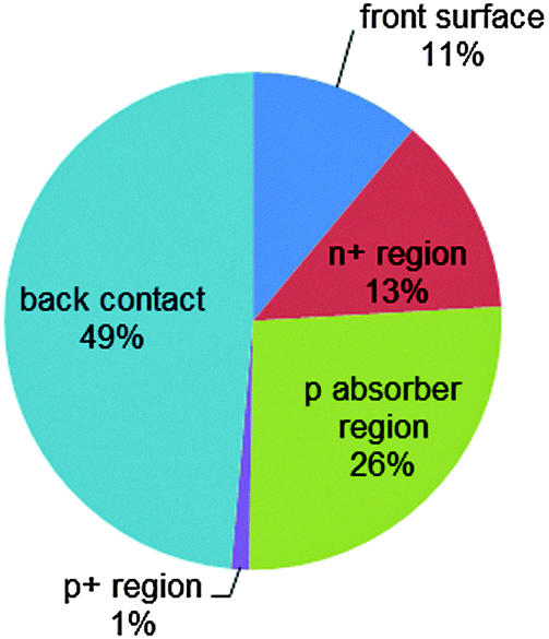
As mentioned above, aluminum-doped regions help to control recombination near the rear metal/semiconductor surface, but they are not ideal from the recombination or optical point of view. The level of recombination current they can achieve is about 1000 fA cm−2, that is, 10 to 50 times larger than a front phosphorus-doped region coated with a passivating dielectric. Hence, they represent a limiting factor to silicon solar cell efficiency.Restricting the aluminum alloyed p+ region to a small fraction (about 1–5%) of the rear surface while passivating the rest with an insulating material has significant electronic and optical benefits. In this approach, which is commonly referred to with the acronyms PERC (Passivated Emitter and Rear Cell), PERL (Passivated Emitter, Rear Locally-doped) or PERT (Passivated Emitter, Rear Totally diffused),1,130 local contact openings (in industry typically as lines) are made in the insulator using, for example, laser ablation (Fig. 6). Subsequently, an aluminum paste is screen printed over the full rear surface and fired, so that local p+ regions are formed within the openings in the dielectric. This approach is similar to so-called laser-fired contacts, where local openings are made after the final rear metallization.32,131 In either case, the result is the formation of an almost ideal back surface mirror, since internal reflection inside the silicon device significantly benefits from the presence of a low refractive index material between the metal and the silicon wafer.132,133 Free-carrier absorption in the classic, uniform p+ aluminum-doped region is also avoided.
 | ||
| Fig. 6 Schematic of the components of a localized rear contact solar cell with dielectric rear surface passivation. Aluminum doping from the back contact into the silicon wafer (green) is confined to the small openings in the rear passivation layer, minimizing recombination. The dielectric passivation layer simultaneously improves the reflectivity of the aluminum back reflector. | ||
But the greatest benefit from the localized contact approach comes from the superior control of surface recombination achievable with insulating films. Arguably the best known among such films is created by high-temperature oxidation of silicon surfaces to form silicon oxide,28 which can yield very low interface state densities,133 combined with a level of charge-assisted passivation.26 Although resulting in low surface recombination velocities, high-temperature thermal oxidation can deteriorate the bulk carrier lifetime due to dissolution of impurity clusters in the multicrystalline material.134 Even if intelligent process sequencing to maximize phosphorus gettering can be used to circumvent the problem, a second high-temperature step can add cost and complexity to solar cell fabrication. Because of that, deposited films are generally preferred in industry to achieve passivation of the rear surface. Hydrogenated amorphous silicon nitride, commonly used at the n+ front, is unsuitable for rear surface passivation in actual solar cells: even though good surface passivation can be obtained on p-type surfaces,135 the presence of such a layer at the rear in solar cells causes undesired shunting at the local rear contacts.136
The search for a suitable dielectric to passivate p-type silicon surfaces has been increasingly intensive since the early 2000s.37,137–141 A breakthrough came with the advent of aluminum oxide, which is a negative fixed-charge dielectric,39,40 essentially avoiding the shunting path caused by silicon nitride in locally contacted solar cells. Such films show a very high negative fixed-charge density (around 1013 cm−2),27 strongly attracting holes to the surface and thus creating a p+ accumulation layer, which helps to suppress electron recombination at the rear surface. Aluminum oxide layers can be deposited with a variety of techniques, including atomic layer deposition,39,40 plasma-enhanced chemical vapor deposition,142,143 atmospheric pressure chemical vapor deposition,144 and sputtering.145 As most of the charges are located very close to the silicon surface, these layers can be kept very thin (a few nanometers), although they are usually capped with a thicker silicon nitride146 or silicon oxide147 layer to improve internal optical reflection in the device. In case no blanket metallization is applied, the developed cells can be used for bifacial applications.70,148 Importantly such stacks can be engineered to withstand contact firing,149–153 To fully exploit the benefit of dielectric-layer integration at the rear of solar cells, it may be desirable to polish the rear side of the silicon wafer.101,154–156 As aluminum oxide is an excellent passivation layer for p-type surfaces, very successful results have also been reported integrating this dielectric at the front, boron-diffused region of n-type solar cells.157
The idea of restricting the contacts to lines or points, while passivating most of the surface with an insulator was applied in 1989 to the rear undiffused side of p-type silicon solar cells in ref. 19 (line contacts, silicon nitride passivation) and in ref. 158 (point contacts, silicon oxide passivation) for small laboratory devices. By adapting and scaling up such concepts, the photovoltaic industry is currently developing similar cell designs.153 A record industrial partial rear contact (PERC/PERL) solar cell on p-type silicon wafers was recently announced by Trina Solar, China, reaching an independently certified efficiency of 22.13% (see Table 1).12,315
3.3. Metallization
The screen-printed silver pastes typically employed by industry need to be subjected to a contact firing step. Besides ensuring a low contact resistance between the metal and the diffused n-type region underneath, the conductivity of the printed lines improves during firing, but remains, nevertheless, higher than that of pure metal lines. This can be resolved with metal plating.159–161 Thanks to the improved line conductivity and the different patterning technique, narrower and taller lines can be fabricated, reducing shading losses. Copper is often the metal of choice, offering attractive cost advantages. Another advantage of this approach is that it circumvents the firing-stability constraint for dielectric passivation layers. High-performance firing-free devices have been reported that exploit firing-incompatible passivation approaches, such as the use of hydrogenated amorphous silicon as rear surface passivating film,139 and hybrid devices featuring a homojunction front contact and a heterojunction rear contact.162,163 Despite these developments, an important breakthrough with direct industrial impact will be the development of a full-area hole-selective passivating rear contact that can withstand the contact firing process.3.4. Wafer crystallinity and conductivity type
In recent years, significant progress has been made in the casting of multicrystalline silicon ingots. Relatively small grain sizes can better accommodate the stress associated with crystallization, thus reducing the density of dislocations inside the grains. This is of great importance, as dislocations are strong recombination sites.164 Moreover, dislocation-rich regions are relatively unresponsive to gettering and hydrogenation treatments.165 The use of this material, called high-performance multicrystalline silicon, is becoming pervasive and is partly responsible for the improved performance now achieved with multicrystalline silicon solar cells.166 Monocrystalline silicon is capable of even higher performance, and further gains may be obtained by changing its conductivity type. As has already been pointed out, p-type wafers have historically dominated over n-type wafers.62 This choice could also be argued to be beneficial from a performance perspective, as the mobility of the minority carrier in the absorber wafer region (i.e., electrons) is about a factor of three higher than that of holes in n-type wafers. This yields much longer diffusion lengths for wafers with identical carrier lifetimes. However, the comparison between p-type and n-type silicon is frequently done at constant resistivity. If the comparison is instead made at equal dopant concentration (which is more meaningful in terms of achievable device voltage), then the Auger limit to the lifetime is higher for p-type crystalline silicon than for n-type crystalline silicon.17 In practice, for wafers with comparable dopant and defect concentrations, the carrier lifetime of n-type silicon is usually much higher than that of p-type silicon.167 One reason for this is that typical carrier lifetime killers in silicon are transition metals,168,169 which generally have much larger carrier capture cross sections for electrons than for holes.170 A second reason is that a significant oxygen concentration is usually present in Czochralski-grown silicon, which is known to lead to the formation of a boron–oxygen complex under light exposure or excess carrier injection,171,172 with a subsequent degradation of the minority-carrier lifetime.173 In comparison, the minority-carrier lifetime of n-type silicon is not affected by the presence of oxygen, and the Czochralski method can be used to grow high-quality ingots.Despite these factors, p-type silicon remains the material of choice for the photovoltaic industry. An important reason for this is to be found in the solidification of silicon from its molten state. Boron has a segregation coefficient close to 1, which results in a small variation of its concentration along the silicon ingot and a relatively tight distribution of wafer resistivity. In contrast, phosphorus has a low segregation coefficient that results in a strong variation of wafer resistivity along the ingot (approximately a factor of 10). Although not insurmountable, it is an obstacle for industrial processes and device designs with tight wafer resistivity specifications.
Yet another reason for the predominance of p-type silicon is the relative simplicity and proven expertise of implementing the thermal diffusion of phosphorus to form the p–n junction on a p-type wafer, compared to the relative novelty and higher temperature of boron diffusion. The traditional n+pp+ firing-through process sequence described in Section 2.2. cannot easily be transferred to n-type wafers. The p+nn+ device structure corresponding to the latter requires both boron and phosphorus diffusions, since an n-type dopant element (donor) that may be alloyed to silicon does not exist. This issue was recently circumvented in a 22.5% device featuring an n+np+ structure, where the p+ region was located at the rear, and where contact firing was replaced by low-temperature copper-plated metallization.160,174
Despite this, the principal advantage of n-type silicon over p-type in terms of resilience to metal contaminants is largely wiped out by the gettering action of the phosphorus diffusion and the aluminum alloying. In this context, the possibility to make high-efficiency diffused-junction solar cells from p-type silicon wafers was recently further underlined by Trina Solar, China, announcing efficiencies of 22.13 and 21.25%, using p-type monocrystalline and multicrystalline wafers, respectively (Table 1). There remains the light-induced degradation caused by boron–oxygen complexes, but a cure for the defect seems to have been found,175 possibly linked to the introduction of hydrogen into the wafer.176 The use of alternative p-dopants, such as gallium, may be a strategy to circumvent this degradation issue,177 provided that homogeneous doping through a full ingot can be established. In either case, the use of high-lifetime wafers with classic device structures such as the so-called aluminum back surface field solar cell would only marginally improve device performance. To better exploit the merits of n-type wafers motivates the introduction of alternative device architectures, of which the two most archetypical are the interdigitated-back-contact solar cell and the heterojunction solar cell.
Finally, as described in Section 2.2, monocrystalline and multicrystalline wafers are obtained from a wire-cutting process, with a typical associated kerf loss of about 100 μm per cut wafer. This explains the quest for “kerf-less” crystalline silicon technologies, including silicon ribbon growth,178,179 film (re-)crystallization,180–182 and silicon epitaxial growth,183–189 possibly combined with lift-off, controlled spalling or other techniques to detach thin silicon absorbers from a thicker substrate190,191 or growth template.192,193 Several strategies have been developed to increase light coupling in ultra-thin silicon (<50 μm) and fabricate solar cells from such material.194–204 In particular Solexel's 239.7 cm2 cell using 35 μm-thick silicon delivered a remarkable power conversion efficiency of 21.2%.11
4. Archetypal high-efficiency concepts
4.1. Interdigitated-back-contact solar cells
Whereas the very first crystalline silicon solar cell, developed at Bell Labs, USA, featured already a back-contact architecture,205,206 the modern interdigitated-back-contact (IBC) cell originally envisioned for applications under concentrated illumination has its origins in the late 1970s.207–209 The first successful commercialization was by SunPower, with a device architecture derived from earlier work at Stanford University.210 With its most recent technological improvements, SunPower has demonstrated an efficiency of 25.2% under one-sun operation.12 A SunPower module has achieved a 22.8% conversion efficiency, which is the current world record for a large-area crystalline silicon photovoltaic module (15![[thin space (1/6-em)]](https://www.rsc.org/images/entities/char_2009.gif) 739 cm2 aperture area; a smaller module with a 778 cm2 designated illumination area by UNSW reached an efficiency of 22.9%, see Fig. 1).12
739 cm2 aperture area; a smaller module with a 778 cm2 designated illumination area by UNSW reached an efficiency of 22.9%, see Fig. 1).12
An important factor for this high performance is the fact that IBC cells achieve high short-circuit currents by completely eliminating metal grid shading at the front surface (Fig. 7). In the IBC design, both electron and hole collection occur at the rear side of the device. This permits a high degree of freedom in the optical and electronic design of the front side of the cell, evidenced by a short-circuit current density as high as 41.33 mA cm−2 for the record IBC cell. Front surface passivation, for example by silicon oxide in combination with silicon nitride as an antireflection layer, can be complemented by a lightly diffused n-type layer, which suppresses the concentration of holes near the pyramidally textured surface. Other possibilities for maximizing light coupling into the wafer include the use of black silicon as a broadband antireflection coating,211–214 and multiscale surface texture.215 Nevertheless, it is essential that such optical schemes be compatible with high-quality surface passivation.
 | ||
| Fig. 7 Schematic of the components of an interdigitated-back-contact cell. Both electrons and holes are extracted through the rear via locally diffused phosphorus and boron stripes that are contacted to individual metal stripes via local openings in the dielectric passivation layer. | ||
In a possible fabrication sequence, boron diffusion is applied to part of the back surface to selectively transport holes. In the remaining part of the back surface, phosphorus is locally diffused to selectively collect electrons. Hence the cell structure consists of alternating, or interdigitated, stripes of n-type and p-type doped regions. Optimization of the widths of the stripes is essential for effective carrier collection and depends on the carrier diffusion length and on the recombination properties of the phosphorus- and boron-doped regions. Since electron mobility is approximately three times higher than hole mobility in moderately doped silicon, some IBC structures favor a one-dimensional flow to holes, by covering a larger fraction of the rear side (for example, around 75%) with a p+ region. This also reduces the buildup of hole concentration at the front surface, which would exacerbate recombination there. Electrons flow mostly laterally towards the n+ rear stripes, not only through the n-type wafer, but also through the front n+ diffusion, when present. Nevertheless, the IBC cell structure needs to be specifically optimized for a given set of recombination and transport properties.
A thin insulating layer is used to passivate the back surface of the wafer.216 Electrical contact is made by metal stripes through local openings etched into the passivation layer. The metal stripes are aligned to the doped regions but they are slightly narrower, to avoid overlap with neighboring stripes, which would cause a shunt. The openings must be large enough to extract current with minimal contact resistance losses and small enough to minimize recombination losses caused by the direct contact of the metal to the silicon. A high fill factor of 82.7% was achieved for the record IBC cell, despite its large area, with this local contact design. A significant advantage of placing both metal contacts at the rear is that they can be optimized without having to trade off resistance for shading. The metal stripes can, in fact, almost fully cover the rear surface, and thus simultaneously act as a back reflector. The thin dielectric layer between the silicon and the metal stripes helps to minimize parasitic plasmonic absorption of infrared light in the metal layer.132
An alternative to minimizing the contact area between the doped silicon and the metal stripes is to incorporate passivating contacts based on doped polysilicon layers,287 which can relax those requirements. With an open-circuit voltage of 737 mV, the record IBC cell demonstrates remarkable bulk lifetime, surface passivation and contact passivation. However, in terms of open-circuit voltage, silicon heterojunction technology can provide even better performance.
4.2. Silicon heterojunction solar cells
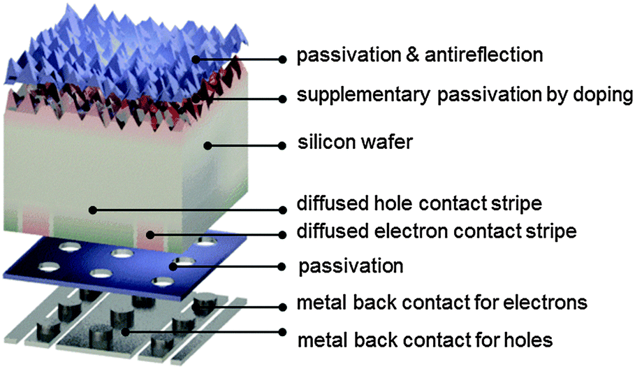
The silicon heterojunction (SHJ) solar cell was pioneered in the early 1990s by Sanyo (acquired in 2010 by Panasonic) and has been commercialized under the HIT trademark (heterojunction with intrinsic thin layer).44,217 Using this concept, Kaneka, Japan, has recently achieved a cell efficiency of 25.1%.370 Panasonic's HIT technology now yields commercial module efficiencies approaching 20%.218 In 2014, Panasonic demonstrated a new world record efficiency of 25.6% by combining their HIT technology with the IBC concept.3 The approximate current density–voltage characteristics of this record cell are compared to the ideal, Auger-limited, solar cell in Fig. 2. The ideality factor and series resistance values for the simulated IBC HIT cell in Fig. 2 were chosen so as to replicate the experimentally measured fill factor of 82.7%. As can be seen in Fig. 2, Jsc and Voc of the record cell are lower than the ideal values, but the largest difference with the ideal limit occurs at the maximum power point. Whereas in the intrinsic limit case the low ideality factor of n = 0.675, typical of Auger recombination in high injection, leads to a very high FF = 89.3%, other recombination mechanisms (probably at the surfaces) at the lower injection conditions of maximum power, or series resistance effects, prevail in the HIT cell and place a cap on the FF.370 In the following we focus on the original two-side contacted silicon heterojunction solar cell.The silicon heterojunction concept is based on two critical innovations. First, it makes use of a thin hydrogenated amorphous silicon layer to achieve excellent surface passivation.42,43,45 To ensure such passivation, it is critical that deposition processes be tuned to obtain atomically sharp interfaces between the wafer and buffer layers, devoid of any unintentionally grown epitaxial silicon.219–222 Second, this thin passivating film is inserted underneath the electron-selective and hole-selective contact layers,44 yielding virtually recombination-free surfaces, even for the areas contacted by the metal electrodes (Fig. 8). This translates into a very high open-circuit voltage,223 with values as high as 750 mV, obtained by Panasonic for a two-side-contacted cell with an efficiency of 24.7%.218 Note that the theoretical, Auger-limited open-circuit voltage for a wafer with similar thickness (∼110 μm), is 761 mV,17,224 underlining the remarkable passivation achieved with this technology.
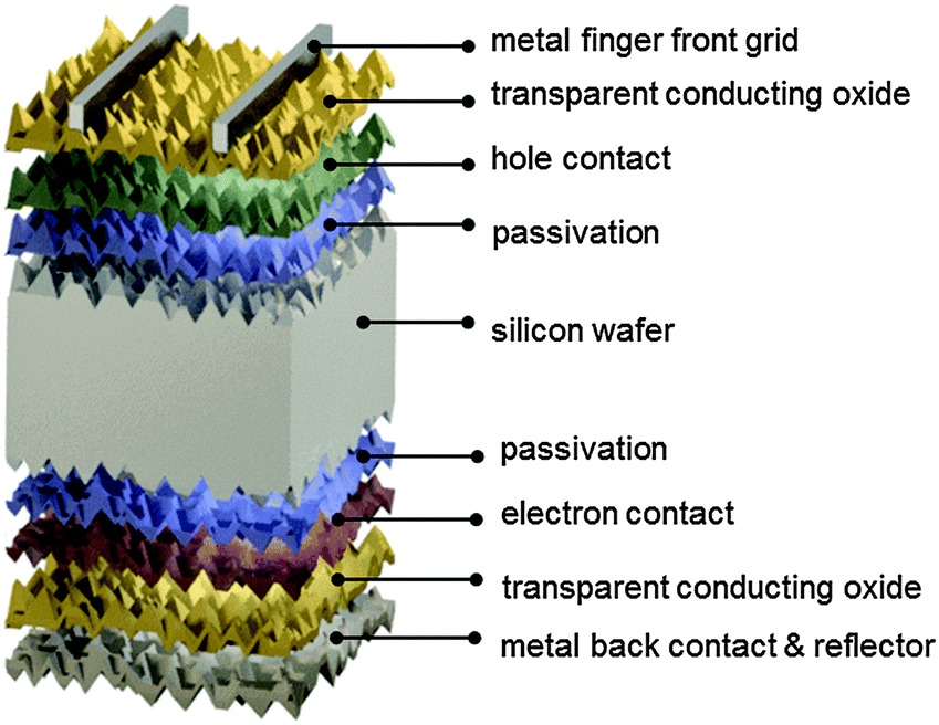 | ||
| Fig. 8 Schematic of the components of a silicon heterojunction cell. The front and rear surfaces of the n-type silicon wafer are passivated by an intrinsic hydrogenated amorphous silicon layer. Contact to holes and electrons is established by subsequently depositing a boron-doped p-type and phosphorus-doped n-type hydrogenated amorphous silicon on the front and rear respectively. Lateral transport of holes at the front to the silver finger grid is achieved employing an indium-oxide-based transparent electrode which simultaneously acts as antireflection coating. A transparent conductive oxide is also employed at the back side to minimize parasitic plasmonic absorption in the silver back reflector. | ||
The fabrication process sequence starts with surface texturing and cleaning, followed by passivation of both sides of the silicon wafer with a thin layer of intrinsic hydrogenated amorphous silicon.46 These films are usually deposited by plasma-enhanced chemical vapor deposition and measure only about 5 nm in thickness.225–227 These films can be considered the “heart” of the silicon heterojunction solar cell, as they yield very effective passivation, while simultaneously being transparent for charge carrier transport. As a consequence, their electronic228–231 and microstructural232,233 properties as well as their deposition processes234–238 have been extensively studied. Rather than relying on dopant diffused regions of the same material (crystalline silicon) to separate the charge carriers, in silicon heterojunction technology such separation is achieved by a combination of doping and use of a wider band gap material, producing nearly ideal carrier-selective contacts. To form these, doped amorphous silicon layers with thicknesses of about 10 nm are deposited on top of the intrinsic layer. Boron is used as a dopant to obtain a p-type layer for transporting the holes, and phosphorus is used to obtain an n-type layer for conducting the electrons. Both dopants are incorporated into the films by adding relevant precursor gasses during film deposition, such as trimethylboron and phosphine. Direct deposition of the doped layers on the crystalline silicon surface degrades passivation, as dopant incorporation generates a significant amount of recombination-active defects in amorphous silicon, explaining the need for intrinsic buffer layers in this technology.239,240 The doped layers may alter the surface passivation when deposited on the intrinsic buffer layers because they can change the carrier concentrations inside the wafer (this is evidenced in Fig. 9 by a bending of the energy bands in equilibrium).241 Interestingly, the silicon heterojunction process sequence can be easily applied to either n-type or p-type wafers,242 with n-type wafers delivering slightly higher efficiencies due to the fact that such surfaces are usually easier to passivate than their p-type counterparts, as discussed above. With this technology it is also fairly straightforward to change the polarity of the device.46,162,243,244 Due to the asymmetric band offsets at the amorphous/crystalline silicon interface, holes usually face a larger barrier than electrons, potentially hindering efficient carrier collection (see Fig. 9).245,246
 | ||
| Fig. 9 Energy band diagram of a silicon heterojunction solar cell in equilibrium showing the valence band offset at the interface between the n-type crystalline silicon (n c-Si) absorber and the intrinsic hydrogenated amorphous silicon passivation layer (i a-Si:H). Representative values were used for the modelling of the curves with the program PC1D66 (n-type wafer doped with 1 × 1015 cm−3 electrons, amorphous silicon with a band gap of 1.8 eV, and electron and hole concentrations of 1 × 1019 cm−3 for n-type and p-type amorphous silicon respectively; for indium tin oxide (ITO), a band gap of 3.3 eV and an electron concentration of 1 × 1021 cm−3 were chosen). Layer thicknesses along the horizontal axis are not to scale, for readability. In particular, the depletion region extends about 1.5 μm into the crystalline silicon wafer. | ||
Full-area contacts are formed by sputtering an indium tin oxide transparent front electrode. As the lateral conductivity of the doped amorphous silicon films is relatively poor, lateral current transport to the metal fingers needs to be provided by the transparent conductive oxide film, requiring a relatively low sheet resistivity of about 50–100 Ω □−1, similar to that of a typical diffused region in classic crystalline silicon solar cells. Thanks to its low refractive index of about 2, this layer is also well suited as an antireflection coating (sometimes in conjunction with a second layer of magnesium difluoride to further minimize reflection losses).60 The transparent conductive oxide is also important to guarantee a sufficiently low contact resistivity, explaining its use at the rear side as well. There, it also helps to reduce parasitic plasmonic absorption of light at the silver back contact, in case this metal is deposited as a blanket layer.132 The cells are finalized by screen printing a silver finger and busbar grid on the front side; copper-plated metallization is an attractive alternative.247–249,370
Compared to the IBC concept, which produces a current density of 41.8 mA cm−2, the silicon heterojunction cell from Kaneka, featuring contacts on opposite sides, delivers a slightly lower short-circuit current density of 40.8 mA cm−2. These losses are caused not only by grid shading, but also by parasitic absorption in the window layers. Optical losses at the front and back surface of silicon heterojunction cells were analyzed in detail in ref. 227 and 250. At the front side, parasitic absorption in the doped and intrinsic amorphous silicon layers with a relatively narrow band gap of about 1.8 eV represents the main contribution to current losses in the blue and ultraviolet part of the spectrum. In the red and infrared part of the spectrum, current is lost mainly through free-carrier absorption in the front and back indium tin oxide electrodes as well as through parasitic plasmonic absorption in the silver back reflector.
Several approaches to improve the short-circuit current of silicon heterojunction cells have been explored, including the replacement of the doped amorphous silicon layers by wider band gap hydrogenated amorphous silicon oxide245,251,252 or silicon carbide layers,253,254 or by replacing the indium tin oxide with higher mobility transparent conductive oxides such as hydrogen-doped indium oxide,255–263 tungsten-doped indium oxide,264 cerium-doped hydrogenated indium oxide,265 and amorphous indium zinc oxide.266 While such transparent conductive oxides clearly lead to an increase in the current density, the use of hydrogenated amorphous silicon oxide or silicon carbide often results in a reduced fill factor, and neutralizes the gains in short-circuit current. In general, fill factor losses related to transparent conductive oxides are due to a suboptimally matched work function,267,268 or to increased sheet or contact resistances between the transparent conductive oxide and the doped amorphous silicon layers.269 Transparent conductive oxides typically exhibit n-type conductivity and consequently readily form an Ohmic contact to n-type hydrogenated amorphous silicon. As p-type transparent conductive oxides suffer from relatively low hole mobilities caused by the large effective hole mass of most oxides,270 contact to p-type amorphous silicon is also commonly established with n-type transparent conductive oxides.271 This recombination junction requires a relatively high carrier concentration in the oxide at least near the interface with p-type amorphous silicon to enable tunneling of carriers across the interface and avoid fill factor losses.259 The deposition process for transparent conductive oxides, such as sputtering, may also lead to undesired performance losses.272 These combined factors motivate the engineering of gently deposited, well-tuned transparent conductive oxides, possibly as multi-layer stacks.273
An alternative approach has made use of a perforated insulating magnesium difluoride layer between the amorphous silicon and transparent indium oxide back electrode, which improves the infrared response significantly as the reflection is increased due to higher refractive index contrast.274 Finally, conformal atomic layer deposition of transparent conducting oxides on black silicon has been demonstrated,275 possibly offering optical advantages. It remains to be seen whether similarly conformal amorphous silicon layers can be produced, yielding efficient devices.
5. Emerging concepts and technologies
5.1. Passivating contacts
As discussed in the previous sections, passivating the two surfaces of the silicon wafer is key to achieving high performance. Ultimately, such passivation should extend to underneath the metal contacts, but, given that most passivating materials are insulators, simultaneously suppressing surface recombination and conducting electrical current is challenging. Silicon heterojunction technology has achieved this, thanks to its use of a semiconductor, intrinsic hydrogenated amorphous silicon, instead of an insulator as the passivating layer. These contacts are somewhat similar to the so-called SIPOS approach – essentially a mixture of microcrystalline silicon and silicon dioxide – which demonstrated Voc values of 720 mV in the mid-1980s.276 The latest IBC cells from SunPower also incorporate an undisclosed passivating contact, yielding open-circuit voltages of up to 737 mV. In this section we describe other possibilities that are based on the use of passivating interlayers thin enough to permit quantum-mechanical tunneling.The idea of using an ultra-thin layer of silicon oxide between metal and semiconductor was exploited in early metal insulator semiconductor (MIS) solar cells277,278 and subsequently applied to devices that had an n–p junction (MINP).279 The use of an ultra-thin film of aluminium oxide deposited by atomic layer deposition onto a phosphorus-diffused region has recently been found to increase the open-circuit voltage by 15 mV, at the expense of a tolerable increase in contact resistance.280,281 Another recent development is an enhanced MIS approach, in which the chemical passivation afforded by a thermal silicon oxide tunnel layer is enhanced by hydrogen originating from a hydrogenated amorphous silicon layer that is carefully alloyed with aluminum.282 This enhanced MIS contact has been applied to the back side of p+nn+ solar cells, which achieved a 21% efficiency.283
Even more effective is to place a ∼1.2 nm-thick silicon oxide layer underneath a ∼30 nm-thick doped polycrystalline (or mixed amorphous/crystalline) silicon film to form what in bipolar transistor technology has been called a polysilicon contact. The thin interlayer can be formed by low-temperature thermal oxidation, immersion in a chemical bath, or by ozone treatment. Selective tunnelling of one type of carrier through the oxide film is required for effective current transport, explaining the need for accurate control of the oxide thickness. The silicon layer is usually deposited by plasma-enhanced chemical vapor deposition, either directly as polycrystalline silicon or as hydrogenated amorphous silicon. Frequently a dopant (phosphorus or boron) is incorporated in situ;284 alternatively, it can be subsequently introduced by ion implantation,285 thermal diffusion from a gaseous source286 or from a doped oxide.287 In all cases, the dopant is activated at a temperature in the range of 800–900 °C, which partially crystallises the initial amorphous silicon layer. Lastly, a hydrogenation treatment, either from a plasma or from annealing in forming gas (i.e. a mixture of nitrogen and hydrogen), is used to further reduce interface recombination. The high temperatures used to form polysilicon contacts makes them, in principle, compatible with the firing-through of a screen-printed front metal grid,288 although it is still unclear if such a process may be applied to the thin polysilicon layer itself. The performance achieved by phosphorus-doped polysilicon contacts is similar to that achieved by the silicon heterojunction technology in terms of recombination current density, which can be as low as J0c ≈ 1–10 fA cm−2, together with contact resistivities approximately one order of magnitude lower than the silicon heterojunction technology, ρc ≈ 20 mΩ cm2.282–284 The application of a tunneling oxide plus an n+ silicon film coated with silver as a full-area rear contact has led to a 25.1% efficient solar cell, using a textured front side, but planar rear side.289 Nevertheless, contacts based on p+ polysilicon seem to be harder to optimize, possibly related to excessively large valence band offsets with the silicon wafer, and their selectivity parameters are not yet as good as those of n+ contacts.290 The 25.1% device mentioned above was made on an n-type silicon wafer that also incorporated a selective boron diffusion on the front surface (heavier under the metal fingers). Similar devices that combine a thermal boron diffusion with a rear n+ polysilicon/silicon oxide contact have been reported recently, albeit with lower efficiencies.8
5.2. Dopant-free electron and hole contacts
All contacting concepts discussed so far employ extrinsic doping as a means to move the Fermi level of the contact region close to the valence or conduction band of the absorber to achieve hole or electron selectivity, respectively. Doping has a number of serious drawbacks. In diffused homojunction cells, heavy doping, which is required to keep the contact resistance to the metal fingers low and consequently to reach high fill factor, leads to Auger recombination, which negatively affects both open-circuit voltage and short-circuit current, in particular the blue response. In silicon heterojunction cells, doping of the amorphous silicon layers creates recombination-active defects that negatively affect passivation, rendering the use of an intrinsic amorphous silicon buffer layer mandatory.240 Again this negatively affects the blue response and, consequently, the short-circuit current, as the band gap of amorphous silicon is only 1.8 eV.250 These shortcomings motivate the search for dopant-free contact concepts compatible with silicon.A glimpse outside silicon photovoltaics proves that doping is not a necessary ingredient for solar cell construction.291 Cadmium telluride (CdTe) thin-film solar cells use a thin, undoped, naturally n-type cadmium sulfide layer with a low carrier concentration,292 deposited typically by chemical bath deposition, as an electron-selective contact. They also use a naturally p-type zinc telluride layer to facilitate hole extraction out of the cadmium telluride absorber layer to the molybdenum metal back contact. A similar strategy is used also for copper indium gallium selenide (CIGS) and copper zinc tin selenide (CZTS) solar cells. As early as 1977, cadmium sulfide was tested as an electron-selective contact to p-type silicon, but efficiencies remained below 10%.293
Dye-sensitized solar cells, in their earliest implementations, used titanium dioxide (TiO2) to extract electrons and the redox potential of a liquid iodide/triiodide electrolyte to extract the holes from a photoexcited dye absorber.294 Titanium dioxide is still a popular electron contact and is also commonly employed for lead halide perovskites295 and even III–V absorbers.296 A heterojunction solar cell employing a p-type silicon absorber with a titanium dioxide electron contact was reported in ref. 297, but suffered from a low open-circuit voltage of 520 mV and, consequently, low efficiency. The application of TiO2 to n-type silicon wafers, motivated by evidence of reasonably good surface passivation,298,299 has been more successful. Recently, a 19.8% efficient n-type silicon solar cell with a front boron diffusion and a rear full-area TiO2 passivating contact has been reported.300 Adding a tunneling silicon oxide layer to the contact structure further reduced recombination, and led to a 20.5% conversion efficiency.301
To extract holes, lead halide perovskite solar cells typically employ a p-type polymer such as 2,2′,7,7′-tetrakis(N,N-di-p-methoxyphenylamine)-9,9′-spirobi-fluorene (spiro-OMeTAD). P-type polymers including spiro-OMeTAD or poly(3,4-ethylenedioxythiophene) polystyrene sulfonate (PEDOT:PSS) have also been employed as hole front contacts for n-type crystalline silicon, and have recently reached an efficiency of 13.8% (see supplementary information in ref. 302 for a compilation of polymer/silicon hybrid cell performance data preceding the cells reported in ref. 303). Nevertheless, their air and ultraviolet stability remains a major concern.304 As an alternative to polymer contact layers, the organic photovoltaic community introduced transition metal oxides as hole-selective contacts. In particular the adoption of substoichiometric molybdenum trioxide (MoOx, x < 3) led to significant improvements in device performance and stability.305,306
The use of substoichiometric molybdenum trioxide (MoOx) as a hole contact for n-type crystalline silicon was first introduced in ref. 302. With its very high work function of up to 6.6 eV, exceeding that of elemental metals, MoOx can act as an efficient hole contact without the use of doping. While the first MoOx–silicon heterojunction cell reached an efficiency of only 14.3%, it already outperformed the best polymer/silicon hybrid cells at that time. Subsequently, an efficiency of 16.4%307 followed by 16.7%308 was achieved for a solar cell made by depositing MoOx directly onto an n-type silicon wafer.
A significant boost in efficiency was achieved by combining the MoOx hole contact with an intrinsic hydrogenated amorphous silicon passivation layer.309 The cell structure is identical to the silicon heterojunction cell discussed in Section 4.2., but replaces the narrow band gap p-type amorphous silicon layer with the wide band gap MoOx (3.3 eV, see Fig. 10), resulting in a substantial current gain of 1.9 mA cm−2, thanks to an improved capture of the blue and ultraviolet region of the spectrum, and a respectable efficiency of 18.8%. Importantly, the open-circuit voltage of this cell was as high as for a co-processed silicon heterojunction reference cell with the standard amorphous silicon layer, demonstrating that MoOx deposition did not deteriorate the surface passivation. However, due to a low fill factor of only 67.2%, the cell efficiency did not exceed the 20% benchmark.
 | ||
| Fig. 10 Energy band diagram of a MoOx–silicon heterojunction solar cell in equilibrium. Comparison with Fig. 9 reveals that n-type MoOx has an effect similar to that of p-type amorphous silicon on band bending in the crystalline silicon absorber due to its high work function. Representative values were used for the modelling of the curves with the program PC1D66 (n-type crystalline silicon wafer doped with 1 × 1015 cm−3 electrons, amorphous silicon with a band gap of 1.8 eV and electron concentration of 1 × 1019 cm−3 for the n-type amorphous silicon; for MoOx and ITO, a band gap of 3.3 eV and an electron concentration of 1 × 10¹⁶ and 1 × 1021 cm−3 were assumed). Layer thicknesses along the horizontal axis are not to scale for readability. In particular, the depletion region extends about 1.5 μm into the crystalline silicon wafer. | ||
The fill factor issue was finally solved in ref. 310, where the annealing temperature after screen printing of the silver finger grid was reduced from 200 to 130 °C. Low-temperature annealing avoids the formation of an interfacial layer between MoOx and the indium oxide transparent electrode, which is believed to be responsible for the low fill factor previously observed. A remarkable fill factor of 80.4% and an independently certified efficiency of 22.5% were finally obtained by replacing the screen-printed finger grid with a copper-plated finger grid, which does not require annealing at 200 °C.310
The use of MoOx as an excellent Ohmic contact to p-type silicon even without a passivation layer was proposed in ref. 311. Contact resistivities as low as 0.2 mΩ cm2 and recombination current densities of 200 fA cm−2 were demonstrated. Consequently, an interesting application of MoOx is as a hole contact at the back of p-type silicon solar cells, where it can replace local p+ regions formed by aluminum alloying or boron diffusion. A proof of concept device with an efficiency of 20.4% has been demonstrated.312 A device employing a PEDOT:PSS full area hole contact at the back of a p-type (n-type) silicon solar cell reached an efficiency of 20.6% (18.3%).313,314 Implementing PEDOT:PSS at the flat back avoids the challenges associated with spin coating on a textured surface and resolves the issue with ultraviolet stability.
6. Summary and outlook
6.1 Summary of silicon solar cells
The rapid progress during the last ten years in the field of silicon photovoltaics has consolidated early laboratory results into large-area, industrially made devices (see Fig. 1). While the fabrication of the 25% efficient, 4 cm2 PERL cell in 1999 cell required several photolithography steps, the photovoltaic industry has adapted the key ingredients of that cell design to large volume production, and Trina Solar has recently reported an independently certified efficiency of 22.13%.12,315 In the meantime, several conceptually very different technologies have managed to reach or cross the 25.0% efficiency barrier (see Table 1). These include Panasonic's 25.6% efficient cell combining the HIT with the IBC approach, SunPower's 25.2% IBC cell, Kaneka's 25.1% silicon heterojunction cell, which tops the 24.7% HIT cell record set by Panasonic in 2012, and Fraunhofer's 25.1% cell featuring a tunneling oxide passivated contact (TOPCon). It is remarkable that with the exception of the 4 cm2 TOPCon cell, all these cells were certified for areas exceeding 100 cm2.From Fig. 1, a similar scenario can be observed for modules. Indeed, while the best module efficiency achieved to date (22.9%, by UNSW) was certified as early as 1996 for a minimodule area of 778 cm2, SunPower has demonstrated an independently certified full-sized 15739 cm2 module with an efficiency of 22.8%.12 Although this review has not described module fabrication technologies, the trends shown in Fig. 1 indicate that it is just a question of time until progress in solar cell performance translates into higher module efficiencies. This applies both to best-of-a-kind modules and to those produced at large scale.316
Two ingredients are necessary at the cell level to achieve high efficiency: an excellent interface passivation scheme and efficient carrier-selective contacts. While classic crystalline silicon solar cells use doping to achieve the latter, several dopant-free concepts have emerged. Molybdenum oxide has been proved to function as a highly efficient hole contact for both n-type and p-type silicon.302,307–310 Such dopant-free contact concepts show great promise for silicon solar cells as a potential route to minimize Auger recombination in the carrier-selective regions. Fully dopant-free silicon solar cells are under development at several research laboratories.317,318 The dopant-free device with the highest reported efficiency, close to 20%,319 uses a molybdenum oxide film as a hole-collecting layer and a stack of lithium fluoride and aluminum as the electron-collecting contact. Underneath both contacts, intrinsic hydrogenated amorphous silicon films are inserted for interface passivation.
It is known, not only from the photovoltaic industry, but also from the semiconductor and battery industries, that it may easily take 10 or 20 years to bring new materials and concepts to the market. In principle, a new concept must offer advantages, not only in terms of the properties of its constituent materials, but also in view of their integration into the device, achievable device performance, manufacturability and yield, operational stability, reliability, and cost. The $/W ratio is still a commonly used metric to quantify the cost vs. output power trade-off of different photovoltaic technologies. In recent years, it has become clear that a more relevant metric is the levelized cost of electricity (LCOE), as photovoltaics are competing against other technologies to provide energy in an economic manner. The LCOE, given in units of $/kW h, takes into account not only the cost to build, but also to operate, a system over its lifetime, divided by the total energy output over that lifetime. It is important to realize that a higher efficiency at the cell level impacts the LCOE positively, with a large leverage, while reducing the cost per cell in a module affects the LCOE only marginally, as the sum of fixed costs associated with the glass, back sheet, junction box and balance of system cost, etc. dominate.320 Consequently, there is an opportunity for new concepts to be economically viable even at higher cost.
6.2 Outlook beyond single-junction solar cells
Ultimately, the efficiency of silicon photovoltaics will be limited by Auger recombination (once all contributions to parasitic light absorption, defect-induced recombination and resistive losses are eliminated) inherent to the operation of silicon absorbers in a single-junction architecture under one-sun illumination. Over the past decades, several advanced concepts have been proposed to overcome the single-junction limit of silicon solar cells. These ideas are often referred to as “third-generation” photovoltaics,321 ultimately aiming to approach the thermodynamic limit of 93%.322 Of the different proposed methods, a few may also hold some promise to enhance the efficiency of single-junction silicon solar cells,323 such as spectral downshifting,324 and up- and down-conversion.325–328 Yet, arguably the most straightforward strategy to significantly boost efficiency is the tandem architecture, where silicon offers a nearly ideal band gap value to act as the bottom cell in a two-subcell configuration with a top cell with an ideal band gap of 1.7–1.8 eV. In a two-terminal tandem device, the total number of incident photons is ideally split equally between the two subcells, so that the number of electron–hole pairs generated in each subcell is the same, resulting in a “matched” photogenerated current density (see Fig. 11).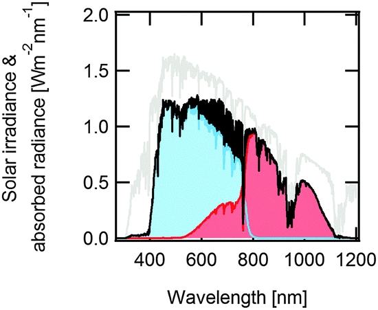 | ||
| Fig. 11 Solar spectral irradiance (air mass 1.5 global spectrum) and contributions absorbed by the top (blue) and bottom cell (red) of a two-terminal perovskite/silicon tandem solar cell.361 The total absorbed radiance includes the black area. | ||
The current density in a tandem is, therefore, half that of a silicon solar cell. The voltage of the two-terminal tandem device is the sum of the voltages of the individual subcells. Given that the material placed on top of the silicon has a wider band gap, it can be expected to produce a higher voltage. Hence the voltage of the tandem cell can be expected to be more than two times higher than the voltage of the single silicon cell, thus resulting in a greater output power. To what extent the voltage, and hence the efficiency, increases depends on technological factors such as interface passivation and contact strategies.
From a pure performance perspective, the most attractive tandem uses a III–V semiconductor solar cell with the appropriate band gap, such as e.g. indium gallium nitride (InGaN) or indium gallium phosphide (InGaP), as the top cell in combination with a silicon bottom cell.329–333 In a four-terminal configuration, efficiencies as high as 29.8% were recently demonstrated for a mechanically stacked III–V/silicon tandem.12 Despite this high efficiency, monolithic two-terminal tandems represent arguably the most elegant tandem design but pose formidable challenges in terms of hetero-epitaxial material growth.334–338 III–V/silicon tandem solar cells fabricated via growth of III–V layer stacks on epitaxial substrates combined with lift-off and layer transfer techniques have been demonstrated, but remain difficult to scale to large volume production.339–343 However, a method for the growth of III–V layers on non-epitaxial substrates has recently been introduced that could change this situation.344,345
A recent analysis revealed that established thin-film technologies based on hydrogenated amorphous silicon or the family of copper indium gallium selenide (CIGS) and copper zinc tin selenide (CZTS) compounds cannot offer a wide band gap top cell with sufficient efficiency to improve or even maintain the efficiency of a >25.0% efficient bottom cell.346 If the silicon cell is dominated by Auger recombination, a halving of the number of photogenerated electrons and holes also implies that its open-circuit voltage gets reduced by 12 mV, compared to full one-sun illumination (18 mV or more if dominated by extrinsic recombination).
A suitable top cell for high-efficiency crystalline silicon bottom cells may be offered by organic–inorganic perovskites.347–349 This material class has only recently been considered for photovoltaic applications, and has achieved a fast progress in device efficiency ever since.350–355 The best single-junction devices use lead-halide-based perovskites as the optical absorber, and have reached efficiencies as high as 21%.356 The band gap of the perovskite absorbers for these single-junction record devices is around 1.57 eV, which is lower than the ideal band gap of 1.7–1.8 eV of a top cell for a silicon-based tandem. Blending lead-iodide-based perovskites with their lead bromide counterparts can open the band gap to the ideal value of 1.7–1.8 eV.357,358 Careful engineering of mixed-cation lead mixed-halide perovskites may resolve the photo-stability issues of wider band gap perovskite absorbers.359 Despite this, using the well-established 1.57 eV band gap lead-iodide-based perovskite can also already be a meaningful approach to significantly boost the efficiency of silicon solar cells; modelling predicts efficiencies of around 30%, largely independent of the precise device design.360 In principle, a four-terminal device offers higher flexibility in device fabrication, as current matching does not need to be respected. However, two-terminal perovskite/silicon tandem solar cells are the most attractive combination of these technologies. The use of a silicon heterojunction solar cell as the bottom cell is particularly attractive.361,362 This demands a perovskite top-cell fabrication process below 200 °C to avoid damage to the bottom cell. With this scheme, monolithic tandem efficiencies of 21% were recently obtained.359 Due to the relatively low refractive index of perovskites,363 the perovskite top cell could act as a “photovoltaic-active” antireflection coating for the bottom silicon solar cell.360 A third possible approach to combine such different technologies is based on spectral splitting technology, with a demonstrated efficiency of 28%.364
The main challenge for tandem architectures is parasitic light absorption,365 for two reasons. Firstly, because of the additional contact (and passivation) layers, additional parasitic absorption is difficult to avoid. Secondly, because the current is cut approximately to half, the overall power conversion efficiency is more strongly affected by optical losses. For example, a 1 mA cm−2 loss in current density due to parasitic absorption in a single-junction crystalline silicon solar cell with 40 mA cm−2 reduces the efficiency by 2.5%, while the same current density loss reduces the efficiency of a two-terminal tandem cell with 20 mA cm−2 by 5%. These arguments hold in particular for perovskite top cells in a tandem architecture; a suitable hole contact layer for perovskite absorbers that overcomes these challenges has yet to be found; the search is ongoing for layers with broadband transparency that are deposited with a process that does not detrimentally affect the underlying layers.366–369 On the other hand, the lower current density of a tandem solar cell should in principle allow for reducing Ohmic losses and indirectly allow for improving the current density, as more resistive contact and passivation layers can be integrated that may offer higher transparency. In addition, the higher voltage in the tandem configuration results in an increased tolerance with respect to slight voltage losses. Nevertheless, perovskite/silicon tandem solar cells that rival single-junction silicon cells have yet to be developed.
This review has focused on recent progress at the solar cell level in the fast-moving field of silicon photovoltaics. Many exciting developments occurring at the module and system levels could not be addressed here, even though they are equally important to ensure the economic competitiveness of solar electricity.
References
- J. H. Zhao, A. H. Wang and M. A. Green, Prog. Photovoltaics, 1999, 7, 471 CAS.
- M. A. Green, Prog. Photovoltaics, 2009, 17, 183 CAS.
- K. Masuko, M. Shigematsu, T. Hashiguchi, D. Fujishima, M. Kai, N. Yoshimura, T. Yamaguchi, Y. Ichihashi, T. Mishima, N. Matsubara, T. Yamanishi, T. Takahama, M. Taguchi, E. Maruyama and S. Okamoto, IEEE J. Photovoltaics, 2014, 4, 1433–1435 CrossRef.
- D. D. Smith, P. Cousins, S. Westberg, R. De Jesus-Tabajonda, G. Aniero and Y.-C. Shen, IEEE J. Photovoltaics, 2014, 4, 1465–1469 CrossRef.
- A. Metz et al., International Technology Roadmap for Photovoltaic, Results 2014, Revision 1, July 2015, http://www.itrpv.net.
- D. M. Powell, M. T. Winkler, H. J. Choi, C. B. Simmons, D. B. Needleman and T. Buonassissi, Energy Environ. Sci., 2012, 5, 5874 Search PubMed.
- A. C. Goodrich, D. M. Powell, T. L. James, M. Woodhouse and T. Buonassisi, Energy Environ. Sci., 2013, 6, 2811 Search PubMed.
- S. W. Glunz, F. Feldmann, A. Richter, M. Bivour, C. Reichel, H. Steinkemper, J. Benick and M. Hermle, Proc. 31st European Photovoltaic Solar Energy Conference and Exhibition, Hamburg, Germany, 2015, p. 363.
- T. Saga, NPG Asia Mater., 2010, 2, 96–102 CrossRef.
- S. Glunz, in Advanced Concepts in Photovoltaics, ed. A. J. Nozik, G. Conibeer and M. C. Beard, Royal Society of Chemistry, Cambridge, 2014 Search PubMed.
- R. Frischknecht, R. Itten, P. Sinha, M. de Wild-Scholten, J. Zhang, V. Fthenakis, H. C. Kim, M. Raugei and M. Stucki, Life Cycle Inventories and Life Cycle Assessment of Photovoltaic Systems, International Energy Agency (IEA) PVPS Task 12, Report T12-04:2015, 2015.
- M. A. Green, K. Emery, Y. Hishikawa, W. Warta and E. D. Dunlop, Prog. Photovoltaics, 2016, 24, 3–11 Search PubMed.
- W. Shockley and H. J. Queisser, J. Appl. Phys., 1961, 32, 510 CrossRef CAS.
- R. M. Swanson, Proc. 31st IEEE Photovoltaic Specialists Conference, Lake Buena Vista, FL, USA, 2005, pp. 889–894.
- A. Richter, S. W. Glunz, F. Werner, J. Schmidt and A. Cuevas, Phys. Rev. B: Condens. Matter Mater. Phys., 2012, 86, 165202 CrossRef.
- M. A. Green, Prog. Photovoltaics, 2002, 10, 235 CAS.
- A. Richter, M. Hermle and S. W. Glunz, IEEE J. Photovoltaics, 2013, 3, 1184–1191 CrossRef.
- S. De Wolf, J. Holovsky, S.-J. Moon, P. Löper, B. Niesen, M. Ledinsky, F.-J. Haug, J.-H. Yum and C. Ballif, J. Phys. Chem. Lett., 2014, 5, 1035–1039 CrossRef CAS PubMed.
- R. Hezel and K. Jaeger, J. Electrochem. Soc., 1989, 136, 518–523 CrossRef CAS.
- A. G. Aberle, Prog. Photovoltaics, 2000, 8, 473 Search PubMed.
- B. S. Richards, Prog. Photovoltaics, 2004, 12, 253 CAS.
- E. Yablonovitch, D. L. Allara, C. C. Chang, T. Gmitter and T. B. Bright, Phys. Rev. Lett., 1986, 57, 249–252 CrossRef CAS PubMed.
- D. B. Fenner, D. K. Biegelsen and R. D. Bringans, J. Appl. Phys., 1989, 66, 419 CrossRef CAS.
- H. S. Higashi, Y. J. Chabal, G. W. Trucks and K. Raghavachari, Appl. Phys. Lett., 1990, 56, 656 CrossRef.
- J. J. Boland, Adv. Phys., 1993, 42, 129 CrossRef CAS.
- S. W. Glunz, D. Biro, S. Rein and W. Warta, J. Appl. Phys., 1999, 86, 683–691 CrossRef CAS.
- B. Hoex, J. J. H. Gielis, M. C. M. van de Sanden and W. M. M. Kessels, J. Appl. Phys., 2008, 104, 113703 CrossRef.
- W. D. Eades and R. M. Swanson, J. Appl. Phys., 1985, 58, 4267 CrossRef CAS.
- E. Yablonovitch, R. M. Swanson, W. D. Eades and B. R. Weinberger, Appl. Phys. Lett., 1986, 48, 245 CrossRef CAS.
- A. G. Aberle, S. Glunz and W. Warta, J. Appl. Phys., 1992, 71, 4422–4431 CrossRef CAS.
- K. Yasutake, Z. Chen, S. K. Pang and A. Rohatgi, J. Appl. Phys., 1994, 75, 2048 CrossRef CAS.
- O. Schultz, S. W. Glunz and G. P. Willeke, Prog. Photovoltaics, 2004, 12, 553–558 CAS.
- T. Lauinger, J. Schmidt, A. G. Aberle and R. Hezel, Appl. Phys. Lett., 1996, 68, 1232–1234 CrossRef CAS.
- M. J. Kerr, J. Schmidt, A. Cuevas and J. H. Bultman, J. Appl. Phys., 2001, 89, 3821–3826 CrossRef CAS.
- H. Mackel and R. Ludemann, J. Appl. Phys., 2002, 92, 2602 CrossRef CAS.
- A. G. Aberle, Sol. Energy Mater. Sol. Cells, 2001, 65, 239 CrossRef CAS.
- I. Martin, M. Vetter, A. Orpella, J. Puigdollers, A. Cuevas and R. Alcubilla, Appl. Phys. Lett., 2001, 79, 2199 CrossRef CAS.
- S. Janz, S. Riepe, M. Hofmann, S. Reber and S. Glunz, Appl. Phys. Lett., 2006, 88, 133516 CrossRef.
- G. Agostinelli, A. Delabie, P. Vitanov, Z. Alexieva, H. F. W. Dekkers, S. De Wolf and G. Beaucarne, Sol. Energy Mater. Sol. Cells, 2006, 90, 3438 CrossRef CAS.
- B. Hoex, S. B. S. Heil, E. Langereis, M. C. M. van de Sanden and W. M. M. Kessels, Appl. Phys. Lett., 2006, 89, 042112 CrossRef.
- G. Dingemans and W. M. M. Kessels, J. Vac. Sci. Technol., A, 2012, 30, 040802 Search PubMed.
- J. I. Pankove and M. L. Tarng, Appl. Phys. Lett., 1979, 34, 156–157 CrossRef CAS.
- S. Olibet, E. Vallat-Sauvain and C. Ballif, Phys. Rev. B: Condens. Matter Mater. Phys., 2007, 76, 035326 CrossRef.
- M. Tanaka, M. Taguchi, T. Matsuyama, T. Sawada, S. Tsuda, S. Nakano, H. Hanafusa and Y. Kuwano, Jpn. J. Appl. Phys., 1992, 31, 3518–3522 CrossRef CAS.
- M. Taguchi, K. Kawamoto, S. Tsuge, T. Baba, H. Sakata, M. Morizane, K. Uchihashi, N. Nakamura, S. Kiyama and O. Oota, Prog. Photovoltaics, 2000, 8, 503–513 CAS.
- S. De Wolf, A. Descoeudres, Z. C. Holman and C. Ballif, Green, 2012, 2, 7 CrossRef CAS.
- K. Misiakos and D. Tsamakis, J. Appl. Phys., 1993, 74, 3293 CrossRef CAS.
- P. Würfel, Physics of Solar Cells: From Principles to New Concepts, Wiley, Weinheim, 2009 Search PubMed.
- O. D. Miller, E. Yablonovitch and S. R. Kurtz, IEEE J. Photovoltaics, 2012, 2, 303–311 CrossRef.
- M. A. Green, J. H. Zhao, A. H. Wang, P. J. Reece and M. Gal, Nature, 2001, 412, 805–808 CrossRef CAS PubMed.
- T. Trupke, M. A. Green, A. Wang, J. Zhao and R. Corkish, J. Appl. Phys., 2003, 94, 4930 CrossRef CAS.
- P. N. Nayak, G. Garcia-Belmonte, A. Kahn, J. Bisquert and D. Cahen, Energy Environ. Sci., 2012, 5, 6022 Search PubMed.
- P. P. Altermatt, J. Schmidt, G. Heiser and A. G. Aberle, J. Appl. Phys., 1997, 82, 4938 CrossRef CAS.
- W. Shockley and W. T. Read, Phys. Rev., 1952, 87, 835–842 CrossRef CAS.
- R. N. Hall, Phys. Rev., 1952, 87, 387 CrossRef CAS.
- A. Cuevas, Energy Procedia, 2014, 55, 53–62 CrossRef.
- D. E. Kane and R. M. Swanson, Proc. 18th IEEE Photovoltaic Specialist Conference, Las Vegas, 1985, p. 578.
- I. Mora-Sero, G. Garcia-Belmonte, P. P. Boix, M. A. Vazquez and J. Bisquert, Energy Environ. Sci., 2009, 2, 678 Search PubMed.
- D. Pysch, A. Mette and S. W. Glunz, Sol. Energy Mater. Sol. Cells, 2007, 91, 1698 CrossRef CAS.
- J. Zhao, A. Wang, P. P. Altermatt and M. A. Green, Appl. Phys. Lett., 1995, 66, 3636 CrossRef CAS.
- H. J. Snaith, Nat. Photonics, 2012, 6, 337 CrossRef CAS.
- J. Mandelkorn, C. McAfee, J. Kesperis, L. Schwartz and W. Pharo, J. Electrochem. Soc., 1962, 109, 313 CrossRef CAS.
- H. Flicker, J. J. Loferski and J. Scott-Monck, Phys. Rev., 1962, 128, 2557 CrossRef CAS.
- J. Mandelkorn and J. H. Lamneck Jr., J. Appl. Phys., 1973, 44, 4785–4787 CrossRef CAS.
- A. Cuevas and D. Yan, IEEE J. Photovoltaics, 2013, 3, 916–923 CrossRef.
- A. Clugston and P. A. Basore, Proc. 26th IEEE Photovoltaic Specialists Conference, Anaheim, CA, USA, 1997, pp. 207–212.
- A. Bidiville, K. Wasmer, M. Van der Meer and C. Ballif, Sol. Energy Mater. Sol. Cells, 2015, 132, 392–402 CrossRef CAS.
- N. Watanabe, Y. Kondo, D. Ide, T. Matsuki, H. Takato and I. Sakata, Prog. Photovoltaics, 2010, 18, 485–490 CAS.
- H. Seingeur, A. Rudack, J. Walters, P. Brooker, K. Davis, W. V. Schoenfeld, S. Raithel, S. Melkote, S. Danyluk, T. Newton, B. Sopori, T. Preece, I. Tarasov, S. Ostapenko, A. Gupto and G. Erfu, Diamond wire sawing for PV – Short- and long-term challenges, March 2015, solarmediastore.com/technical papers.
- K. A. Munzer, K. T. Holdermann, R. E. Schlosser and R. Sterk, IEEE Trans. Electron Devices, 1999, 48, 2055 CrossRef.
- M. A. Green, Adv. Mater., 2001, 13, 1019 CrossRef CAS.
- D. Sarti and R. Einhaus, Sol. Energy Mater. Sol. Cells, 2002, 72, 27–40 CrossRef CAS.
- B. Terheiden, T. Ballman, R. Horbelt, Y. Schiele, S. Seren, J. Ebser, G. Hahn, V. Mertens, M. B. Koentopp, M. Scherff, J. W. Müller, Z. C. Holman, A. Descoeudres, S. De Wolf, S. Martin de Nicolas, J. Geissbuehler, C. Ballif, B. Weber, P. Saint-Cast, M. Rauer, C. Schmiga, S. W. Glunz, D. J. Morrison, S. Devenport, D. Antonelli, C. Busto, F. Grasso, F. Ferrazza, E. Tonelli and W. Oswald, Phys. Status Solidi A, 2015, 212, 13–24 CrossRef CAS.
- E. Vazsonyi, K. De Clercq, R. Einhaus, E. Van Kerschaver, K. Said, J. Poortmans, J. Szlufcik and J. Nijs, Sol. Energy Mater. Sol. Cells, 1999, 57, 179–188 CrossRef CAS.
- K. E. Bean, IEEE Trans. Electron Devices, 1978, 25, 1185 CrossRef.
- P. Campbell and M. A. Green, J. Appl. Phys., 1987, 62, 243 CrossRef.
- R. Einhaus, E. Vazsonyi, J. Szlufcik, J. Nijs and R. Mertens, Proc. 26th IEEE PV Specialists Conference, Anaheim, CA, USA, 1997, p. 167.
- Y. Nishimoto, T. Ishihara and K. Namba, J. Electrochem. Soc., 1999, 146, 457–461 CrossRef CAS.
- J. Szlufcik, F. Duerinckx, J. Horzel, E. Van Kerschaver, H. Dekkers, S. De Wolf, P. Choulat, C. Allebe and J. Nijs, Sol. Energy Mater. Sol. Cells, 2002, 74, 155 CrossRef CAS.
- D. H. Macdonald, A. Cuevas, M. J. Kerr, C. Samundsett, D. Ruby, S. Winderbaum and A. Leo, Sol. Energy, 2004, 76, 277–283 CrossRef CAS.
- S. C. Baker-Finch, K. R. McIntosh and M. L. Terry, IEEE J. Photovoltaics, 2012, 2, 457 CrossRef.
- H. Sai, Y. Kanamori, K. Arafune, Y. Oshita and M. Yamaguchi, Prog. Photovoltaics, 2007, 15, 415 Search PubMed.
- X. Ye, S. Zou, K. Chen, J. Li, J. Huang, F. Cao, X. Wang, L. Zhang, X.-F. Wang, M. Shen and X. Su, Adv. Funct. Mater., 2014, 24, 6708 CrossRef CAS.
- W. Kern, J. Electrochem. Soc., 1990, 137, 1887 CrossRef CAS.
- J. Delalamo, S. Swirhun and R. M. Swanson, Solid-State Electron., 1985, 28, 47 CrossRef CAS.
- R. R. King, R. A. Sinton and R. M. Swanson, IEEE Trans. Electron Devices, 1990, 37, 365 CrossRef CAS.
- P. P. Altermatt, J. O. Schumacher, A. Cuevas, M. J. Kerr, S. W. Glunz, R. R. King, G. Heiser and A. Schenk, J. Appl. Phys., 2002, 92, 3187 CrossRef CAS.
- F. A. Kröger, G. Diemer and H. A. Klasens, Phys. Rev., 1956, 103, 279 CrossRef.
- W. M. Loh, S. E. Swirhun, T. A. Schreyer, R. M. Swanson and K. C. Saraswat, IEEE Trans. Electron Devices, 1987, 34, 512 CrossRef.
- J. R. Davis, A. Rohatgi, R. H. Hopkins, P. D. Blais, P. Raichoudhury, J. R. McCormick and H. C. Mollenkopf, IEEE Trans. Electron Devices, 1980, 27, 667 CrossRef.
- A. A. Istratov, H. Hieslmair and E. R. Weber, Appl. Phys. A: Mater. Sci. Process., 2000, 70, 489 CrossRef CAS.
- G. Coletti, P. C. P. Bronsveld, G. Hahn, W. Warta, D. Macdonald, B. Ceccaroli, K. Wambach, N. Le Quang and J. M. Fernandez, Adv. Funct. Mater., 2011, 21, 879 CrossRef CAS.
- J. S. Kang and D. K. Schroder, J. Appl. Phys., 1989, 65, 2974 CrossRef CAS.
- S. M. Myers, M. Seibt and W. Schroter, J. Appl. Phys., 2000, 88, 3795 CrossRef CAS.
- D. Macdonald, H. Mäckel and A. Cuevas, Appl. Phys. Lett., 2006, 88, 092105 CrossRef.
- J. H. Zhao, A. H. Wang, P. P. Altermatt, S. R. Wenham and M. A. Green, Sol. Energy Mater. Sol. Cells, 1995, 41, 87 Search PubMed.
- H. K. Raut, V. A. Ganesh, A. S. Nair and S. Ramakrishna, Energy Environ. Sci., 2011, 4, 3779 Search PubMed.
- J. Zhao and M. A. Green, IEEE Trans. Electron Devices, 1991, 38, 1925 CrossRef CAS.
- P. Doshi, G. E. Jellison and A. Rohatgi, Appl. Opt., 1997, 36, 7826 CrossRef CAS PubMed.
- F. W. Sexton, Sol. Energy Mater., 1982, 7, 1 CrossRef CAS.
- C. Leguijt, P. Lolgen, J. A. Eikelboom, A. W. Weeber, F. M. Schuurmans, W. C. Sinke, P. F. A. Alkemade, P. M. Sarro, C. H. M. Maree and L. A. Verhoef, Sol. Energy Mater. Sol. Cells, 1996, 40, 297 CrossRef CAS.
- S. De Wolf, G. Agostinelli, G. Beaucarne and P. Vitanov, J. Appl. Phys., 2005, 97, 063305 CrossRef.
- H. F. W. Dekkers, S. De Wolf, G. Agostinelli, F. Duerinckx and G. Beaucarne, Sol. Energy Mater. Sol. Cells, 2006, 90, 3244–3250 CrossRef CAS.
- C. S. Seager, D. S. Ginley and J. D. Zook, Appl. Phys. Lett., 1980, 36, 831 CrossRef CAS.
- F. Duerinckx and J. Szlufcik, Sol. Energy Mater. Sol. Cells, 2002, 72, 231 CrossRef CAS.
- W. Soppe, H. Rieffe and A. Weeber, Prog. Photovoltaics, 2005, 13, 551–569 CAS.
- T. Nunoi, N. Nishimura, T. Nammori, H. Sawai and A. Suzuki, Jpn. J. Appl. Phys., 1980, 19, 67 CrossRef CAS.
- C. Ballif, D. M. Huljic, G. Willeke and A. Hessler-Wyser, Appl. Phys. Lett., 2003, 82, 1878 CrossRef CAS.
- M. M. Hilali, S. Sridharan, C. Khadilkra, A. Shaikh, A. Rohatgi and S. Kim, J. Electron. Mater., 2006, 35, 2041 CrossRef CAS.
- G. Schubert, F. Huster and P. Fath, Sol. Energy Mater. Sol. Cells, 2006, 90, 3399–3406 CrossRef CAS.
- G. C. Cheek, R. P. Mertens, R. Vanoverstraeten and L. Frisson, IEEE Trans. Electron Devices, 1984, 31, 602–609 CrossRef.
- S. Narasimha, A. Rohatgi and A. W. Weeber, IEEE Trans. Electron Devices, 1999, 46, 1363–1370 CrossRef CAS.
- M. Horteis, T. Gutberlet, A. Reller and S. W. Glunz, Adv. Funct. Mater., 2010, 20, 476 CrossRef.
- P. Lauwers, J. Van Meerbergen, P. Bulteel, R. Mertens and R. Van Overstraeten, Solid-State Electron., 1978, 21, 747 CrossRef CAS.
- J. G. Fossum, F. A. Lindholm and M. A. Shibib, IEEE Trans. Electron Devices, 1979, 26, 1294 CrossRef.
- M. A. Shibib, F. A. Lindholm and J. G. Fossum, IEEE Trans. Electron Devices, 1979, 26, 1104 CrossRef.
- R. Woehl, P. Gundel, J. Krause, K. Ruehle, F. D. Heinz, M. Rauer, C. Schmiga, M. C. Schubert, W. Warta and D. Biro, IEEE Trans. Electron Devices, 2011, 58, 441 CrossRef CAS.
- M. Cudzinovic and B. Sopori, Proc. 25th IEEE Photovoltaic Specialists Conference, Washington, DC, USA, 1996, pp. 501–503.
- D. Kray, M. Hermle and S. W. Glunz, Prog. Photovoltaics, 2008, 16, 1–15 CAS.
- Z. C. Holman, M. Filipic, B. Lipovsek, S. De Wolf, F. Smole, M. Topic and C. Ballif, Sol. Energy Mater. Sol. Cells, 2014, 120, 426 CrossRef CAS.
- http://pv.energytrend.com/research/Cost_and_Efficiency_Are_Keys_to_Mono_Si_Market_Growth_in_2016.html, accessed on January 17, 2016.
- S. Philipps and W. Warmuth, Photovoltaic Report, August 2015, http://www.ise.fraunhofer.de.
- http://www.bherenewables.com/include/pdf/fact_sheet_solar_star.pdf, October 2015.
- J. Szlufcik, H. E. Elgamel, M. Ghannam, J. Nijs and R. Mertens, Appl. Phys. Lett., 1991, 59, 1583–1584 CrossRef CAS.
- D. Kray, A. Fell, S. Hopman, K. Mayer, G. P. Willeke and S. W. Glunz, Appl. Phys. A: Mater. Sci. Process., 2008, 93, 99 CrossRef CAS.
- A. Rohatgi, D. L. Meier, B. McPherson, Y. W. Ok, A. D. Upadhaya, J. H. Lay and F. Zimbardi, Energy Procedia, 2012, 15, 10–19 CrossRef CAS.
- Z. Wang, P. Han, H. Lu, H. Qian, L. Chen, Q. Meng, N. Tang, F. Gao, Y. Jiang, J. Wu, W. Wu, H. Zhu, J. Ji, Z. Shi, A. Sugianto, L. Mai, B. Hallam and S. Wenham, Prog. Photovoltaics, 2012, 20, 260 CAS.
- G. Hahn, Proc. 25th European Photovoltaic Energy Conference and Exhibition/5th World Conference on Photovoltaic Energy Conversion, Valencia, Spain, 2010, pp. 1091–1096.
- T. C. Roder, S. J. Eisele, P. Grabitz, C. Wagner, G. Kulushich, J. R. Kohler and J. H. Werner, Prog. Photovoltaics, 2010, 18, 505–510 Search PubMed.
- M. A. Green, Sol. Energy Mater. Sol. Cells, 2015, 143, 190 CrossRef CAS.
- E. Schneiderlöchner, R. Preu, R. Lüdemann and S. W. Glunz, Prog. Photovoltaics, 2002, 10, 29 Search PubMed.
- Z. C. Holman, S. De Wolf and C. Ballif, Light: Sci. Appl., 2013, 2, e106 CrossRef.
- L. M. Terman, Solid-State Electron., 1962, 5, 285 CrossRef CAS.
- T. Buonassisi, A. I. Istratov, M. A. Marcus, B. Lai, Z. Cai, S. M. Heald and E. R. Weber, Nat. Mater., 2005, 4, 676 CrossRef CAS PubMed.
- A. G. Aberle and R. Hezel, Prog. Photovoltaics, 1997, 5, 29 CAS.
- S. Dauwe, L. Mittelstadt, A. Metz and R. Hezel, Prog. Photovoltaics, 2002, 19, 271 Search PubMed.
- A. Rohatgi, P. Doshi, J. Moschner, T. Lauinger, A. G. Aberle and D. S. Ruby, IEEE Trans. Electron Devices, 2000, 47, 987 CrossRef CAS.
- M. Hofmann, S. Janz, C. Schmidt, S. Kambor, D. Suwito, N. Kohn, J. Rentsch, R. Preu and S. W. Glunz, Sol. Energy Mater. Sol. Cells, 2009, 93, 1074 CrossRef CAS.
- M. Schaper, J. Schmidt, H. Plagwitz and R. Brendel, Prog. Photovoltaics, 2005, 13, 381–386 CAS.
- P. Vitanov, G. Agostinelli, A. Harizanova, T. Ivanova, M. Vukadinovic, N. Le Quang and G. Beaucarne, Sol. Energy Mater. Sol. Cells, 2006, 90, 2489 CrossRef CAS.
- O. Schultz, A. Mette, M. Hermle and S. W. Glunz, Prog. Photovoltaics, 2008, 16, 317 CAS.
- P. Saint-Cast, D. Kania, M. Hofmann, J. Benick, J. Rentsch and R. Preu, Appl. Phys. Lett., 2009, 95, 151502 CrossRef.
- P. Saint-Cast, J. Benick, D. Kania, L. Weiss, M. Hofmann, J. Rentsch, R. Preu and S. W. Glunz, IEEE Electron Device Lett., 2010, 31, 695 CrossRef CAS.
- L. E. Black and K. R. McIntosh, Appl. Phys. Lett., 2012, 100, 202107 CrossRef.
- T. T. Li and A. Cuevas, Phys. Status Solidi RRL, 2009, 3, 160 CrossRef CAS.
- J. Schmidt, B. Veith and R. Brendel, Phys. Status Solidi RRL, 2009, 3, 287 CrossRef CAS.
- A. Uruena, M. Aleman, E. Cornagliotti, J. Deckers, M. Haslinger, L. Tous, R. Russell, J. John, Y. Yao, T. Soderstrom, F. Duerinckx and J. Szlufcik, presented at the European PV Solar Energy Conference and Exhibition, September 2015, Hamburg, Germany.
- A. Hubner, A. G. Aberle and R. Hezel, Appl. Phys. Lett., 1997, 70, 1008 CrossRef CAS.
- J. Benick, A. Richter, M. Hermle and S. W. Glunz, Phys. Status Solidi RRL, 2009, 3, 233–235 CrossRef CAS.
- S. Gatz, H. Hannebauer, R. Hesse, F. Werner, A. Schmidt, T. Dullweber, J. Schmidt, K. Bothe and R. Brendel, Phys. Status Solidi RRL, 2011, 5, 147 CrossRef CAS.
- B. Vermang, H. Goverde, L. Tous, A. Lorenz, P. Choulat, J. Horzel, J. John, J. Poortmans and R. Mertens, Prog. Photovoltaics, 2012, 20, 269–273 CAS.
- M. Moors, K. Baert, T. Caremans, F. Duerinckx, A. Cacciato and J. Szlufcik, Sol. Energy Mater. Sol. Cells, 2012, 106, 84 CrossRef CAS.
- A. Metz, D. Adler, S. Bagus, H. Blanke, M. Bothar, E. Brouwer, S. Dauwe, K. Dresser, R. Droessler, T. Droste, M. Fiedler, Y. Gassenbauer, T. Grahl, N. Hermert, W. Kuzminski, A. Lachowicz, T. Launinger, N. Lenck, M. Manole, M. Martini, R. Messmer, C. Meyer, J. Moschner, K. Ramspeck, P. Roth, R. Schönfelder, B. Schum, J. Sticksel, K. Vaas, M. Volk and K. Wangemann, Sol. Energy Mater. Sol. Cells, 2014, 120, 417 CrossRef CAS.
- E. Cornagliotti, A. Uruena, J. Horzel, J. John, L. Tous, D. Hendrickx, V. Prajapati, S. Singh, R. Hoyer, F. Delahaye, K. Weise, D. Queisser, H. Nussbaumer and J. Poortmans, Proc. 27th European Photovoltaic Solar Energy Conference and Exhibition, Frankfurt, Germany, 2012, p. 561.
- C. Schwab, A. Wolf, M. Graf, N. Wohrle, S. Kuhnhold, J. Greulich, G. Kastner, M. Zimmer, D. Biro and R. Preu, IEEE J. Photovoltaics, 2013, 3, 613 CrossRef.
- M. Richter, P. Saint-Cast, T. Dannenberg, M. Zimmer and J. Rentsch, Energy Procedia, 2015, 77, 832 CrossRef CAS.
- J. Benick, B. Hoex, M. C. M. Van de Sanden, W. M. M. Kessels, O. Schultz and S. W. Glunz, Appl. Phys. Lett., 2008, 92, 253504 CrossRef.
- A. W. Blakers, A. Wang, A. M. Milne, J. Zhao and M. Green, Appl. Phys. Lett., 1989, 55, 1363 CrossRef CAS.
- Z. Wang, P. Han, H. Lu, H. Qian, L. Chen, Q. Meng, N. Tang, F. Gao, Y. Jiang, J. Wu, W. Wu, H. Zhu, J. Ji, Z. Shi, A. Sugianto, L. Mai, B. Hallam and S. Wenham, Prog. Photovoltaics, 2012, 20, 260 CAS.
- L. Tous, M. Aleman, R. Russell, E. Cornagliotti, P. Choulat, A. Uruena, S. Singh, J. John, F. Duerinckx, J. Poortmans and R. Mertens, Prog. Photovoltaics, 2015, 23, 660–670 CAS.
- J. Horzel, Y. Shengzhao, N. Bay, M. Passig, D. Pysch, H. Kühnlein, H. Nussbaumer and P. Verlinden, IEEE J. Photovoltaics, 2015, 6, 1595–1600 CrossRef.
- M. Bivour, C. Reichel, M. Hermle and S. W. Glunz, Sol. Energy Mater. Sol. Cells, 2012, 106, 11–16 CrossRef CAS.
- L. Tous, S. N. Granata, A. Rouhi, J. F. Lerat, T. Emeraud, S. M. de Nicolas, T. M. Pletzer, R. Labie, M. Aleman, R. Russell, J. John, F. Duerinckx, J. Szlufcik, S. De Wolf, C. Ballif, R. Mertens and J. Poortmans, Energy Procedia, 2014, 55, 715–723 CrossRef CAS.
- C. Hassler, G. Stollwerck, W. Koch, W. Krumbe, A. Muller, D. Franke and T. Rettelbach, Adv. Mater., 2001, 13, 1815 CrossRef CAS.
- A. Bentzen, A. Holt, R. Kopecek, G. Stokkan, J. S. Christensen and B. G. Svenson, J. Appl. Phys., 2006, 99, 093509 CrossRef.
- Y. M. Yang, A. Yu, B. Hsu, W. C. Hsu, A. Yang and C. W. Lan, Prog. Photovoltaics, 2015, 23, 340–351 CAS.
- J. E. Cotter, J. H. Guo, P. J. Cousins, M. D. Abbott, F. W. Chen and K. C. Fisher, IEEE Trans. Electron Devices, 2006, 53, 1893–1901 CrossRef CAS.
- D. Macdonald, A. Cuevas, A. Kinomura, Y. Nakano and L. J. Geerligs, J. Appl. Phys., 2005, 97, 033523 CrossRef.
- T. Buonassisi, A. A. Istratov, M. D. Picket, M. Heuer, J. P. Kalejs, G. Hahn, M. A. Marcus, B. Lai, Z. Cai, S. M. Heald, T. F. Ciszek, R. F. Clark, D. W. Cunningham, A. M. Gabor, R. Jonczyk, S. Narayanan, E. Sauar and E. R. Weber, Prog. Photovoltaics, 2006, 14, 513–531 CAS.
- D. Macdonald and R. J. Geerligs, Appl. Phys. Lett., 2004, 85, 4061 CrossRef CAS.
- S. W. Glunz, S. Rein, J. Y. Lee and W. Warta, J. Appl. Phys., 2001, 90, 2397–2404 CrossRef CAS.
- J. Schmidt and K. Bothe, Phys. Rev. B: Condens. Matter Mater. Phys., 2004, 69, 024107 CrossRef.
- S. W. Glunz, S. Rein, W. Warta, J. Knobloch and W. Wettling, Sol. Energy Mater. Sol. Cells, 2001, 99, 219 CrossRef.
- M. Recaman Payo, I. Kuzma-Filipek, F. Duercinkx, Y. Li, E. Cornagliotti, A. Uruena, A. Sharma, L. Tous, A. Sharma, A. Hajjiah and J. Poortmans, presented at the European PV Solar Energy Conference and Exhibition, September 2015, Hamburg, Germany.
- A. Herguth, G. Schubert, M. Kaes and G. Hahn, Prog. Photovoltaics, 2008, 16, 135–140 CAS.
- S. Wilking, A. Herguth and G. Hahn, J. Appl. Phys., 2013, 113, 194503 CrossRef.
- S. W. Glunz, S. Rein, J. Knobloch, W. Wettling and T. Abe, Prog. Photovoltaics, 1999, 7, 463 CAS.
- J. I. Hanoka, Sol. Energy Mater. Sol. Cells, 2001, 65, 231 CrossRef CAS.
- J. P. Kalejs, Sol. Energy Mater. Sol. Cells, 2002, 72, 139 CrossRef CAS.
- M. J. McCann, K. R. Catchpole, K. J. Weber and A. W. Blakers, Sol. Energy Mater. Sol. Cells, 2001, 68, 135 CrossRef CAS.
- O. Nast, S. Brehme, S. Pritchard, A. G. Aberle and S. R. Wenham, Sol. Energy Mater. Sol. Cells, 2001, 65, 385–392 CrossRef CAS.
- J. Haschke, D. Amkreutz, L. Korte, F. Ruske and B. Rech, Sol. Energy Mater. Sol. Cells, 2014, 128, 190–197 CrossRef CAS.
- J. H. Petermann, D. Zielke, J. Schmidt, F. Haase, E. G. Rojas and R. Brendel, Prog. Photovoltaics, 2012, 20, 1–5 CAS.
- C. W. Teplin, M. P. Paranthaman, T. R. Fanning, K. Alberi, L. Heatherly, S. H. Wee, K. Kim, F. A. List, J. Pineau, J. Bornstein, K. Bowers, D. F. Lee, C. Cantoni, S. Hane, P. Schroeter, D. L. Young, E. Iwanicko, K. M. Jones and H. M. Branz, Energy Environ. Sci., 2011, 4, 3346–3350 Search PubMed.
- S. H. Wee, C. Cantoni, T. R. Fanning, C. W. Teplin, D. F. Bogorin, J. Bornstein, K. Bowers, P. Schroeter, F. Hasoon, H. M. Branz, M. P. Paranthamanan and A. Goyal, Energy Environ. Sci., 2012, 5, 6052–6056 Search PubMed.
- B. Demaurex, R. Bartlome, J. P. Seif, J. Geissbuhler, D. T. L. Alexander, Q. Jeangros, C. Ballif and S. De Wolf, J. Appl. Phys., 2014, 116, 053519 CrossRef.
- N. Milenkovic, T. Rachow, S. Janz and S. Reber, Energy Procedia, 2015, 77, 613 CrossRef CAS.
- C. W. Teplin, S. Grover, A. Chitu, A. Limanov, M. Chahal, J. Im, D. Amkreutz, S. Gall, H. P. Yoon, V. Lasalvia, P. Stradins, K. M. Jones, A. G. Norman, D. L. Young, H. M. Branz and B. G. Lee, Prog. Photovoltaics, 2015, 23, 909–915 CAS.
- E. Kobayashi, Y. Watabe, R. Hao and T. S. Ravi, Appl. Phys. Lett., 2015, 106, 223504 CrossRef.
- V. Depauw, Y. Qiu, K. Van Nieuwenhuysen, I. Gordon and J. Poortmans, Prog. Photovoltaics, 2011, 19, 844–850 CAS.
- R. Martini, S. Granata, V. Depauw, M. Gonzales, I. Goron and J. Poortmans, Energy Procedia, 2014, 55, 879–884 CrossRef CAS.
- F. Dross, K. Baert, T. Bearda, J. Deckers, V. Depauw, O. El Daif, I. Gordon, A. Gougam, J. Govaerts, S. Granata, R. Labie, X. Loozen, R. Martini, A. Masolin, B. O'Sullivan, Y. Qui, J. Vaes, D. Van Gestel, J. Van Hoeymissen, A. Vanleenhove, K. Van Nieuwenhuysen, S. Venkatachalam, M. Meuris and J. Poortmans, Prog. Photovoltaics, 2012, 20, 770–784 CAS.
- I. Gordon, F. Dross, V. Depauw, A. Masolin, Y. Qiu, Y. Vaes, D. Van Gestel and J. Poortmans, Sol. Energy Mater. Sol. Cells, 2011, 95, S2–S7 CrossRef CAS.
- A. Wang, J. Zhao, S. R. Wenham and M. A. Green, Prog. Photovoltaics, 1996, 4, 55–58 CAS.
- V. Depauw, I. Gordon, G. Beaucarne, J. Poortmans, R. Mertens and J. P. Celis, Phys. Status Solidi C, 2009, 6, 1750–1753 CrossRef CAS.
- J. Yoon, A. J. Baca, S.-I. Park, P. Elvikis, J. G. Geddess Ill, L. Li, R. H. Kim, J. Xiao, S. Wang, T.-H. Kim, M. J. Motala, B. Y. Ahn, E. B. Duoss, J. A. Lewis, R. G. Nuzzo, P. M. Ferreira, Y. Huang, A. Rockett and J. A. Rogers, Nat. Mater., 2008, 7, 907 CrossRef CAS PubMed.
- R. A. Rao, L. Mathew, S. Saha, S. Smith, D. Sarkar, R. Garcia, R. Stout, A. Gurmu, E. Onyegam, D. Ahn, D. Xu, D. Jawarani, J. Fossum and S. Banerjee, Proc. 37st IEEE Photovoltaic Specialists Conference, Seattle, WA, USA, 2011, pp. 001504–001507.
- J. L. Cruz-Campa, G. N. Nielson, P. J. Resnick, C. A. Sanchez, P. J. Clews, M. Okandan, T. Friedmann and V. P. Gupta, IEEE J. Photovoltaics, 2011, 1, 3–8 CrossRef.
- D. Jawarani, D. Xu, S. Smith, R. A. Rao, L. Mathew, S. Saha, D. Sarkar, S. Banerjee and P. S. Ho, Proc. 38st IEEE Photovoltaic Specialists Conference, Austin, TX, USA, 2012, vol. 2, pp. 1–4.
- S. W. Bedell, D. Shahrjerdi, B. Hekmatshoar, K. Fogel, P. A. Lauro, J. A. Ott, N. Sosa and D. Sadana, IEEE J. Photovoltaics, 2012, 2, 141–147 CrossRef.
- S. Jeong, M. D. McGehee and Y. Cui, Nat. Commun., 2013, 4, 2950 Search PubMed.
- L. Wang, A. Lochtefeld, J. Han, A. P. Gerger, M. Carroll, J. Ji, A. Lennon, H. Li, R. Opila and A. Barnett, IEEE J. Photovoltaics, 2014, 4, 1397 CrossRef.
- A. Ignenito, O. Isabella and M. Zeman, ACS Photonics, 2014, 3, 270 Search PubMed.
- C.-C. Lin, Y.-J. Chuang, W.-H. Sun, C. Cheng, Y.-T. Chen, Z.-L. Chen, C.-H. Chien and F.-H. Ko, Microelectron. Eng., 2015, 145, 128–132 CrossRef CAS.
- D. M. Chapin, C. S. Fuller and G. L. Pearson, J. Appl. Phys., 1954, 25, 676 CrossRef CAS.
- L. L. Kazmerski, J. Electron Spectrosc. Relat. Phenom., 2006, 150, 105 CrossRef CAS.
- M. D. Lammert and R. J. Schwartz, IEEE Trans. Electron Devices, 1977, 24, 338 CrossRef.
- R. M. Swanson, Prog. Photovoltaics, 2000, 8, 93 CAS.
- E. Van Kerschaver and G. Beaucarne, Prog. Photovoltaics, 2006, 14, 107 Search PubMed.
- R. A. Sinton, Y. Kwark, J. Y. Gan and R. M. Swanson, IEEE Electron Device Lett., 1986, 7, 567 CrossRef.
- H. C. Yuan, V. E. Yost, M. R. Page, P. Stradins, D. L. Meier and H. M. Branz, Appl. Phys. Lett., 2009, 95, 123501 CrossRef.
- X. G. Liu, P. R. Coxon, M. Peters, B. Hoex, J. M. Cole and D. J. Fray, Energy Environ. Sci., 2014, 7, 3223 Search PubMed.
- M. Otto, M. Algasinger, H. Branz, B. Gesemann, T. Gimpel, K. Fuchsel, T. Kasebier, S. Kontermann, S. Koynov, X. P. Li, V. Naumann, J. Oh, A. N. Sprafke, J. Ziegler, M. Zilk and R. B. Wehrspohn, Adv. Opt. Mater., 2015, 3, 147 CrossRef CAS.
- H. Savin, P. Repo, G. V. Gastrow, P. Ortega, E. Calle, M. Garin and R. Alcubilla, Nat. Nanotechnol., 2015, 10, 624 CrossRef CAS PubMed.
- A. Ingenito, O. Isabella and M. Zeman, Prog. Photovoltaics, 2015, 23, 1649 CAS.
- W. P. Mulligan, D. H. Rose, M. J. Cudzinovic, D. M. De Ceuster, K. R. McIntosh, D. D. Smith and R. Swanson, Proc. 19th European Photovoltaics Solar Energy Conference, Paris, France, 2014, pp. 387–390.
- M. Taguchi, M. Tanaka, T. Matsuyama, T. Matsuoka, S. Tsuda, S. Nakano, Y. Kishi and Y. Kuwano, Tech. Digest 5th International Photovoltaic Science and Engineering Conference, Kyoto, Japan, 1990, p. 689.
- M. Taguchi, A. Yano, S. Tohoda, K. Matsuyama, T. Nishikawa, K. Fujita and E. Maruyama, IEEE J. Photovoltaics, 2014, 4, 96 CrossRef.
- T. H. Wang, E. Iwaniczko, M. R. Page, D. H. Levi, Y. Yan, H. M. Branz and Q. Wang, Thin Solid Films, 2006, 501, 284 CrossRef CAS.
- H. Fujiwara and M. Kondo, Appl. Phys. Lett., 2007, 90, 013503 CrossRef.
- S. De Wolf and M. Kondo, Appl. Phys. Lett., 2007, 90, 042111 CrossRef.
- Y. F. Yang, M. Page, T. H. Wang, M. M. Al-Jassim, H. M. Branz and Q. Wang, Appl. Phys. Lett., 2006, 88, 121925 CrossRef.
- M. Taguchi, A. Terakawa, E. Maruyama and M. Tanaka, Prog. Photovoltaics, 2005, 13, 481 CAS.
- T. Tiedje, E. Yablonovitch, G. D. Cody and B. G. Brooks, IEEE Trans. Electron Devices, 1984, 31, 711 CrossRef.
- M. Taguchi, E. Maruyama and M. Tanaka, Jpn. J. Appl. Phys., 2008, 47, 814 CrossRef CAS.
- H. Fujiwara and M. Kondo, J. Appl. Phys., 2007, 101, 054516 CrossRef.
- Z. C. Holman, A. Descoeudres, L. Barraud, F. Z. Fernandez, J. P. Seif, S. De Wolf and C. Ballif, IEEE J. Photovoltaics, 2012, 2, 7–15 CrossRef.
- T. F. Schulze, L. Korte, F. Ruske and B. Rech, Phys. Rev. B: Condens. Matter Mater. Phys., 2011, 83, 165314 CrossRef.
- S. De Wolf, B. Demaurex, A. Descoeudres and C. Ballif, Phys. Rev. B: Condens. Matter Mater. Phys., 2011, 83, 233301 CrossRef.
- S. De Wolf, C. Ballif and M. Kondo, Phys. Rev. B: Condens. Matter Mater. Phys., 2012, 85, 113302 CrossRef.
- B. M. George, J. Behrends, A. Schnegg, T. F. Schulze, M. Fehr, L. Korte, B. Rech, K. Lips, M. Rohrmüller, E. Rauls, W. G. Schmidt and U. Gerstmann, Phys. Rev. Lett., 2013, 110, 136803 CrossRef CAS PubMed.
- T. F. Schulze, H. N. Beushausen, C. Leendertz, A. Dobrich, B. Rech and L. Korte, Appl. Phys. Lett., 2010, 96, 252102 CrossRef.
- J. Holovsky, S. De Wolf, P. Jiricek and C. Ballif, Rev. Sci. Instrum., 2015, 86, 073108 CrossRef PubMed.
- H. Fujiwara and M. Kondo, Appl. Phys. Lett., 2005, 86, 032112 CrossRef.
- A. Descoeudres, L. Barraud, S. De Wolf, B. Strahm, D. Lachenal, C. Guerin, Z. C. Holman, F. Zicarelli, B. Demaurex, J. P. Seif, J. Holovsky and C. Ballif, Appl. Phys. Lett., 2011, 99, 123506 CrossRef.
- J. Geissbuhler, S. De Wolf, B. Demaurex, J. P. Seif, D. T. L. Alexander, L. Barraud and C. Ballif, Appl. Phys. Lett., 2013, 23, 231604 CrossRef.
- R. Bartlome, S. De Wolf, B. Demaurex, C. Ballif, E. Amanatides and D. Mataras, J. Appl. Phys., 2015, 117, 203303 CrossRef.
- J. J. H. Gielis, P. J. van den Oever, B. Hoex, M. C. M. van de Sanden and W. M. M. Kessels, Phys. Rev. B: Condens. Matter Mater. Phys., 2008, 77, 205329 CrossRef.
- L. Korte and M. Schmidt, J. Non-Cryst. Solids, 2008, 354, 2138 CrossRef CAS.
- S. De Wolf and M. Kondo, J. Appl. Phys., 2009, 105, 103707 CrossRef.
- C. Leendertz, N. Mingirulli, T. F. Schulze, J. P. Kleider, B. Rech and L. Korte, Appl. Phys. Lett., 2011, 98, 2108 CrossRef.
- A. Descoeudres, Z. C. Holman, L. Barraud, S. Morel, S. De Wolf and C. Ballif, IEEE J. Photovoltaics, 2013, 3, 1–7 CrossRef.
- M. Bivour, S. Schroer, M. Hermle and S. W. Glunz, Sol. Energy Mater. Sol. Cells, 2014, 122, 120–129 CrossRef CAS.
- R. Varache, O. N. Aguila, A. Valla, N. Nguyen and D. Munoz, IEEE J. Photovoltaics, 2015, 5, 711–717 CrossRef.
- J. P. Seif, A. Descoeudres, M. Filipic, F. Smole, M. Topic, Z. C. Holman, S. De Wolf and C. Ballif, J. Appl. Phys., 2014, 115, 0245502 CrossRef.
- M. Mews, M. Liebhaber, B. Rech and L. Korte, Appl. Phys. Lett., 2015, 107, 013902 CrossRef.
- J. Geissbuehler, S. De Wolf, A. Faes, N. Badel, Q. Jeangros, A. Tomasi, L. Barraud, A. Descoeudres, M. Despeisse and C. Ballif, IEEE J. Photovoltaics, 2014, 4, 1055–1062 CrossRef.
- J. B. Heng, J. M. Fu, B. Kong, Y. Chae, W. Wang, Z. G. Xie, A. Reddy, K. Lam, C. Beitel, C. Liao, C. Erben, Z. Q. Huang and Z. Xu, IEEE J. Photovoltaics, 2015, 5, 82 CrossRef.
- L. Tous, S. N. Granata, P. Choulat, T. Bearda, A. Michel, A. Uruena, E. Cornagliotti, M. Aleman, R. Gehlaar, R. Russell, F. Duerinckx and J. Szlufcik, Sol. Energy Mater. Sol. Cells, 2015, 142, 66 CrossRef CAS.
- Z. C. Holman, M. Filipic, A. Descoeudres, S. De Wolf, F. Smole and C. Ballif, J. Appl. Phys., 2013, 113, 013107 CrossRef.
- T. Mueller, S. Schwertheim, M. Scherff and W. R. Fahrner, Appl. Phys. Lett., 2008, 92, 33504 CrossRef.
- L. Mazarella, S. Kirner, B. Stannowski, L. Korte, B. Rech and R. Schlatmann, Appl. Phys. Lett., 2015, 106, 023902 CrossRef.
- T. Mueller, W. Duengen, Y. Ma, R. Job, M. Scherr and W. R. Fahrner, J. Appl. Phys., 2007, 102, 4505 CrossRef.
- M. Boccard and Z. C. Holman, J. Appl. Phys., 2015, 118, 065704 CrossRef.
- T. Koida, H. Fujiwara and M. Kondo, Jpn. J. Appl. Phys., 2007, 46, L685 CrossRef CAS.
- T. Koida, H. Fujiwara and M. Kondo, Appl. Phys. Express, 2008, 1, 041501 CrossRef.
- C. Battaglia, L. Erni, M. Boccard, L. Barraud, J. Escarré, K. Söderström, G. Bugnon, A. Billet, L. Ding, M. Despeisse, F.-J. Haug, S. De Wolf and C. Ballif, J. Appl. Phys., 2011, 109, 114501 CrossRef.
- J. A. Libera, J. N. Hryn and J. W. Elam, Chem. Mater., 2011, 23, 2150–2158 CrossRef CAS.
- L. Barraud, Z. C. Holman, N. Badel, P. Reiss, A. Descoeudres, C. Battaglia, S. De Wolf and C. Ballif, Sol. Energy Mater. Sol. Cells, 2013, 115, 151 CrossRef CAS.
- B. Macco, H. C. M. Knoops and W. M. M. Kessels, ACS Appl. Mater. Interfaces, 2015, 7, 16723 Search PubMed.
- S. Limpijumnong, P. Reunchan, A. Janotti and C. G. Van de Walle, Phys. Rev. B: Condens. Matter Mater. Phys., 2009, 80, 193202 CrossRef.
- N. Preissler, O. Bierwagen, A. T. Ramu and J. S. Speck, Phys. Rev. B: Condens. Matter Mater. Phys., 2013, 88, 085305 CrossRef.
- H. Scherg-Kurmes, S. Körner, S. Ring, M. Klaus, L. Korte, F. Ruske, R. Schlatmann, B. Rech and B. Szyszka, Thin Solid Films, 2015, 594, 316–322 CrossRef CAS.
- F. Meng, J. Shi, Z. Liu, Y. Cui, Z. Lu and Z. Feng, Sol. Energy Mater. Sol. Cells, 2014, 122, 70 CrossRef CAS.
- E. Kobayashi, Y. Watabe and T. Yamamoto, Appl. Phys. Express, 2015, 8, 015505 CrossRef.
- M. Morales-Masis, S. Martin de Nicolas, J. Holovsky, S. De Wolf and C. Ballif, IEEE J. Photovoltaics, 2015, 5, 1340 CrossRef.
- R. Rössler, C. Leendertz, L. Korte, N. Mingirulli and B. Rech, J. Appl. Phys., 2013, 113, 144513 CrossRef.
- A. Tomasi, F. Sahli, J. P. Seif, L. Fanni, S. Martin de Nicolas, J. Geissbuehler, B. Paviet-Salomon, S. Nicolay, L. Barraud, B. Niesen, S. De Wolf and C. Ballif, IEEE J. Photovoltaics, 2016, 6, 17 CrossRef.
- A. Tomasi, B. Paviet-Salomon, D. Lachenal, S. Martin de Nicolas, A. Descoeudres, J. Geissbuehler, S. De Wolf and C. Ballif, IEEE J. Photovoltaics, 2014, 4, 1046 CrossRef.
- G. Hautier, A. Miglio, G. Ceder, G.-M. Rignanese and X. Gonze, Nat. Commun., 2013, 4, 2292 Search PubMed.
- M. Bivour, S. Schröer and M. Hermle, Energy Procedia, 2013, 38, 658–669 CrossRef CAS.
- B. Demaurex, S. De Wolf, A. Descoeudres, Z. C. Holman and C. Ballif, Appl. Phys. Lett., 2012, 101, 171604 CrossRef.
- B. Demaurex, J. P. Seif, S. Smit, B. Macco, W. M. M. Kessels, J. Geissbuehler, S. De Wolf and C. Ballif, IEEE J. Photovoltaics, 2014, 4, 1387 CrossRef.
- Z. C. Holman, A. Descoeudres, S. De Wolf and C. Ballif, IEEE J. Photovoltaics, 2013, 3, 1243 CrossRef.
- M. Otto, M. Kroll, T. Kaesebier, S. M. Lee, M. Putkonen, R. Salzer, P. T. Miclea and R. B. Wehrspohn, Adv. Mater., 2010, 22, 5035 CrossRef CAS PubMed.
- E. Yablonovitch, T. Gmitter, R. M. Swanson and Y. H. Kwark, Appl. Phys. Lett., 1985, 47, 1211 CrossRef CAS.
- S. J. Fonash, J. Appl. Phys., 1975, 46, 1286 CrossRef.
- R. B. Godfrey and M. A. Green, Appl. Phys. Lett., 1979, 34, 790–793 CrossRef CAS.
- M. A. Green, A. W. Blakers, M. R. Willison, T. Szpitalak, E. M. Keller, E. Gauja and P. J. Hart, Proc. 15th IEEE Photovoltaic Specialists Conference, Orlando, FL, USA, 1981, p. 1405.
- D. Zielke, J. H. Petermann, F. Werner, B. Veith, R. Brendel and J. Schmidt, Phys. Status Solidi RRL, 2011, 5, 298–300 CrossRef CAS.
- J. Bullock, D. Yan and A. Cuevas, Phys. Status Solidi RRL, 2013, 7, 946–949 CrossRef CAS.
- J. Bullock, D. Yan, Y. Wan, A. Cuevas, B. Demaurex, A. Hessler-Wyser and S. De Wolf, J. Appl. Phys., 2014, 115, 163703 CrossRef.
- J. Bullock, A. Cuevas, C. Samundsett, D. Yan, J. McKeon and Y. Wan, Sol. Energy Mater. Sol. Cells, 2015, 138, 22–25 CrossRef CAS.
- F. Feldmann, M. Bivour, C. Reichel, M. Hermle and S. W. Glunz, Sol. Energy Mater. Sol. Cells, 2014, 120, 270–274 CrossRef CAS.
- U. Romer, R. Peibst, T. Ohrdes, B. Lim, J. Krugener, T. Wietler and R. Brendel, IEEE J. Photovoltaics, 2015, 5, 507–514 CrossRef.
- D. Yan, A. Cuevas, J. Bullock, Y. Wan and C. Samundsett, Sol. Energy Mater. Sol. Cells, 2015, 142, 75 CrossRef CAS.
- R. M. Swanson, Back side contact solar cell with doped polysilicon regions, US Pat., 7633006 B1, 2009 Search PubMed.
- A. D. Upadhyaya, Y. W. Ok, E. Chang, V. Upadhyaya, K. Madani, K. Tate, B. Rounsaville, C. J. Choi, V. Chandrasekaran, V. Yelundur, A. Gupta and A. Rohatgi, IEEE J. Photovoltaics, 2016, 6, 153 CrossRef.
- A. Moldovon, F. Feldmann, M. Zimmer, J. Rentsch, J. Benick and M. Hermle, Sol. Energy Mater. Sol. Cells, 2015, 142, 123–127 CrossRef.
- F. Feldmann, M. Simon, M. Bivour, C. Reichel, M. Hermle and S. W. Glunz, Appl. Phys. Lett., 2014, 104, 181105 CrossRef.
- U. Würfel, A. Cuevas and P. Würfel, IEEE J. Photovoltaics, 2015, 5, 461 CrossRef.
- H. Khallaf, I. O. Oladeji, G. Chai and L. Chow, Thin Solid Films, 2008, 516, 7306–7312 CrossRef CAS.
- F. M. Livingstone, W. M. Tsang, A. J. Barlos, R. M. De La Rue and W. Duncan, J. Phys. D: Appl. Phys., 1977, 10, 1959 CrossRef CAS.
- B. O'Regan and M. Grätzel, Nature, 1991, 353, 737–740 CrossRef.
- M. Liu, M. B. Johnston and H. Snaith, Nature, 2013, 501, 395–398 CrossRef CAS PubMed.
- X. Yin, C. Battaglia, Y. Lin, K. Chen, M. Hettick, M. Zheng, C.-Y. Chen, D. Kiriya and A. Javey, ACS Photonics, 2014, 1, 1245–1250 CrossRef CAS PubMed.
- S. Avasthi, W. E. McCain, G. Man, A. Kahn, J. Schwartz and J. Sturm, Appl. Phys. Lett., 2013, 102, 203901 CrossRef.
- B. C. Liao, B. Hoex, A. G. Aberle, D. Z. Chi and C. S. Bhatia, Appl. Phys. Lett., 2014, 104, 253903 CrossRef.
- G. Sahasrabudhe, S. M. Rupich, J. Jhaveri, A. H. Berg, K. A. Nagamatsu, G. Man, Y. J. Chabal, A. Kahn, S. Wagner, J. C. Sturm and J. Schwartz, J. Am. Chem. Soc., 2015, 137, 14842 CrossRef CAS PubMed.
- X. Yang and K. Weber, presented at the 42nd IEEE Photovoltaic Specialist Conference, New Orleans, LA, USA, 2015.
- X. Yang, P. Zheng, Q. Bi and K. Weber, Silicon heterojunction solar cells with electron selective TiOx contact, Sol. Energy Mater. Sol. Cells Search PubMed , accepted for publication.
- C. Battaglia, Y. Yin, M. Zheng, I. D. Sharp, T. Chen, S. McDonnell, A. Azcatl, C. Carraro, B. Ma, R. Maboudian, R. M. Wallace and A. Javey, Nano Lett., 2014, 14, 967–971 CrossRef CAS PubMed.
- R. Liu, S.-T. Lee and B. Sun, Adv. Mater., 2014, 26, 6007 CrossRef CAS PubMed.
- M. Jorgensen, K. Norman and F. C. Krebs, Sol. Energy Mater. Sol. Cells, 2008, 92, 686–714 CrossRef.
- S. Tokito, K. Noda and Y. Taga, J. Phys. D: Appl. Phys., 1996, 29, 2750 CrossRef CAS.
- J. Meyer, S. Hamwi, M. Kröger, W. Kowalsky, T. Riedl and A. Kahn, Adv. Mater., 2012, 24, 5408–5427 CrossRef CAS PubMed.
- L. Ding and M. I. Bertoni, presented at the Materials Research Society, spring meeting, San Francisco, CA, USA, 2015.
- J. Bullock, D. Yan, A. Cuevas, Y. Wan and C. Samundsett, Energy Procedia, 2015, 77, 446 CrossRef CAS.
- C. Battaglia, S. Martin de Nicolas, S. De Wolf, X. Yin, M. Zheng, C. Ballif and A. Javey, Appl. Phys. Lett., 2014, 104, 113902 CrossRef.
- J. Geissbühler, J. Werner, S. Martin de Nicolas, L. Barraud, A. Hessler-Wyser, M. Despeise, S. Nicolay, A. Tomasi, B. Niesen, S. De Wolf and C. Ballif, Appl. Phys. Lett., 2015, 107, 081601 CrossRef.
- J. Bullock, A. Cuevas, T. Allen and C. Battaglia, Appl. Phys. Lett., 2014, 105, 232109 CrossRef.
- J. Bullock, C. Samundsett, A. Cuevas, D. Yan, Y. Wan and T. Allen, IEEE J. Photovoltaics, 2015, 5, 1591–1594 CrossRef.
- J. Schmidt, D. Zielke, W. Lövenich, M. Hörteis and A. Elschner, Proc. 6th World Conference on Photovoltaic Energy Conversion, 6TUO.15.6, Kyoto, Japan, 2014.
- D. Zielke, C. Niehaves, W. Lövenich, A. Elschner, M. Hörteis and J. Schmidt, Energy Procedia, 2015, 77, 331–339 CrossRef CAS.
- http://ir.trinasolar.com/phoenix.zhtml?c=206405&p=irol-newsArticle&ID=2122938, accessed on January 17, 2016.
- M. A. Green, Nat. Energy, 2015, 1, 15015 CrossRef.
- K. A. Nagamatsu, S. Avasthi, G. Sahasrabudhe, G. Man, J. Jhaveri, A. H. Berg, J. Schwartz, A. Kahn, S. Wagner and J. C. Sturm, Appl. Phys. Lett., 2015, 106, 123906 CrossRef.
- Y. Zhang, W. Cui, Y. Zhu, F. Zu, L. Liao, S. T. Lee and B. Sun, Energy Environ. Sci., 2015, 8, 297 Search PubMed.
- J. Bullock, M. Hettick, J. Geissbühler, A. J. Ong, T. Allen, C. M. Sutter-Fella, T. Chen, H. Ota, E. T. Schaler, S. De Wolf, C. Ballif, A. Cuevas and A. Javey, Nat. Energy, 2016, 2, 15031 CrossRef.
- A. Hauser, A. Richter and S. Leu, Cell and module design from the LCOE perspective, October 2015, http://www.meyerburger.com/fileadmin/user_upload/meyerburger.com/Downloads/Publikationen/Dokumente/2014_PV_Annual_LCOE.pdf.
- In this philosophy, the first and second generations are crystalline silicon and thin-film semiconductor based photovoltaics, respectively.
- M. A. Green, Prog. Photovoltaics, 2001, 9, 123–135 CAS.
- C. Strumpel, M. McCann, G. Beaucarne, V. Arkhipov, A. Slaoui, V. Svrcek, C. del Canizo and I. Tobias, Sol. Energy Mater. Sol. Cells, 2006, 91, 238–249 CrossRef.
- W. G. J. H. M. van Sark, A. Meijerink, R. E. I. Schropp, J. A. M. van Roosmalen and E. H. Lysen, Sol. Energy Mater. Sol. Cells, 2005, 87, 395–409 CrossRef CAS.
- T. Trupke, M. A. Green and P. Wurfel, J. Appl. Phys., 2002, 92, 4117 CrossRef CAS.
- A. Shalav, B. S. Richards, T. Trupke, K. W. Kramer and H. U. Gudel, Appl. Phys. Lett., 2005, 86, 013505 CrossRef.
- A. Shalav, B. S. Richards and M. A. Green, Sol. Energy Mater. Sol. Cells, 2007, 91, 829 CrossRef CAS.
- S. Fischer, J. C. Goldschmidt, P. Löper, G. H. Bauer, R. Bruggemann, K. Kramer, D. Biner, M. Hermle and S. W. Glunz, J. Appl. Phys., 2010, 108, 044912 CrossRef.
- Y. Komatsu, T. Fuyuki and H. Matsunami, Jpn. J. Appl. Phys., 1996, 35, 4389 CrossRef CAS.
- L. Hsu and W. Walukiewicz, J. Appl. Phys., 2008, 104, 024507 CrossRef.
- S. Essig, S. Ward, M. A. Steiner, D. J. Friedman, J. F. Geisz, P. Stradins and D. L. Young, Energy Procedia, 2015, 77, 464–469 CrossRef CAS.
- J. M. Zahler, K. Tanabe, C. Ladous, T. Pinnington, F. D. Newman and H. Atwater, Appl. Phys. Lett., 2007, 91, 012108 CrossRef.
- S. Essig, J. Benick, M. Schachtner, A. Wekkeli, M. Hermle and F. Dimroth, IEEE J. Photovoltaics, 2015, 5, 977 CrossRef.
- T. Soga, K. Baskar, T. Kato, T. Jimbo and M. Umeno, J. Cryst. Growth, 1997, 174, 579 CrossRef CAS.
- L. A. Reichertz, I. Gherasoiu, K. M. Yu, V. M. Kao, W. Walukiewicz and J. W. Ager, Appl. Phys. Express, 2009, 2, 122202 CrossRef.
- F. Dimroth, T. Roesener, S. Essig. C. Weuffen, A. Wekkeli, E. Oliva, G. Siefer, K. Volz, T. Hannappel, D. Häussler, W. Jäger and A. W. Bett, IEEE J. Photovoltaics, 2014, 4, 620 CrossRef.
- I. Gherasoiu, K. M. Yu, L. A. Reichertz, V. M. Kao, M. Hawkridge, J. W. Ager and W. Walukiewicz, Phys. Status Solidi B, 2010, 247, 1747–1749 CrossRef CAS.
- T. J. Grassman, D. J. Chmielewski, S. D. Carnevale, J. A. Carlin and S. A. Ringel, IEEE J. Photovoltaics, 2016, 6, 326 CrossRef.
- K. Tanabe, K. Watanabe and Y. Arakawa, Sci. Rep., 2012, 2, 349 CrossRef PubMed.
- K. Derendorf, S. Essig, E. Oliva, V. Klinger, T. Roesener, S. P. Phillips, J. Benick, M. Hermle, M. Schachtner, G. Siefer, W. Jager and F. Dimroth, IEEE J. Photovoltaics, 2013, 3, 1423–1428 CrossRef.
- A. C. Tamboli, M. F. A. M. van Hest, M. A. Steiner, S. Essig, E. E. A. G. Norman, N. Bosco and P. Stradins, Appl. Phys. Lett., 2015, 106, 263904 CrossRef.
- A. Meijer, M. A. J. Huijbregts, J. J. Schemer and L. Reijnders, Prog. Photovoltaics, 2003, 11, 275–287 CAS.
- A. Fontcuberta i Morral, J. M. Zahler, H. A. Atwater, S. P. Ahrenkeil and M. W. Wanlass, Appl. Phys. Lett., 2003, 83, 5413 CrossRef CAS.
- R. Kapadia, Z. Yu, H.-H. H. Wang, M. Zheng, C. Battaglia, M. Hettick, D. Kiriya, K. Takei, P. Lobaccaro, J. W. Beeman, J. W. Ager, R. Maboudian, D. C. Chrzan and A. Javey, Sci. Rep., 2013, 3, 2275 CrossRef PubMed.
- M. Zheng, H. P. Wang, C. M. Sutter-Fella, C. Battaglia, S. Aloni, X. Wang, J. Moore, J. W. Beeman, M. Hettick, M. Amani, W. T. Hsu, J. W. Ager, P. Bermel, M. Lundstrom, H. He and A. Javey, Adv. Energy Mater., 2015, 5, 1501337 CrossRef.
- T. P. White, N. N. Lal and K. R. Catchpole, IEEE J. Photovoltaics, 2014, 4, 208–214 CrossRef.
- P. F. H. Löper, B. Niesen, S.-J. Moon, S. Martin de Nicolas, Z. Remes, J. Holovsky, Z. Remes, M. Ledinsky, F.-J. Haug, J.-H. Yum, S. De Wolf and C. Ballif, IEEE J. Photovoltaics, 2014, 4, 154 CrossRef.
- N. N. Lal, T. P. White and K. R. Catchpole, IEEE J. Photovoltaics, 2014, 4, 1380 CrossRef.
- M. A. Green, A. Ho-Baillie and H. J. Snaith, Nat. Photonics, 2014, 8, 506 CrossRef CAS.
- A. Kojima, K. Teshima, Y. Shirai and T. Miyasaka, J. Am. Chem. Soc., 2009, 131, 6050 CrossRef CAS PubMed.
- H. S. Kim, C. R. Lee, J. H. Im, K. B. Lee, T. Moehl, A. Marchioro, S. J. Moon, R. Humphry-Baker, J. H. Yum, J. E. Moser, M. Gratzel and N. G. Park, Sci. Rep., 2012, 2, 591 CrossRef PubMed.
- M. M. Lee, J. Teuscher, T. Miyasaka, T. N. Murakami and H. J. Snaith, Science, 2012, 338, 643 CrossRef CAS PubMed.
- J. Burschka, N. Pellet, S. J. Moon, R. Humphry-Baker, P. Gao, M. K. Nazeeruddin and M. Gratzel, Nature, 2013, 499, 316 CrossRef CAS PubMed.
- H. P. Zhou, Q. Chen, G. Li, S. Luo, T. B. Song, H. S. Duan, Z. R. Hong, J. B. You, Y. S. Liu and Y. Yang, Science, 2014, 345, 542 CrossRef CAS PubMed.
- W. S. Yang, J. H. Noh, N. J. Jeon, Y. C. Kim, S. Ryu, J. Seo and S. I. Seok, Science, 2015, 348, 1234 CrossRef CAS PubMed.
- Dyesol, Media Release, 8 December 2015.
- J. H. Noh, S. H. Im, J. H. Heo, T. N. Mandal and S. I. Seok, Nano Lett., 2013, 13, 1764 CrossRef CAS PubMed.
- A. Sadhanala, F. Deschler, T. H. Thomas, S. E. Dutton, K. C. Goedel, F. C. Hanusch, M. L. Lai, U. Steiner, T. Bein, P. Docampo, D. Cahen and R. H. Friend, J. Phys. Chem. Lett., 2014, 5, 2501 CrossRef CAS PubMed.
- D. P. Mc Meekin, G. Sadoughi, W. Rehman, G. E. Eperon, M. Saliba, M. T. Hörantner, A. Haghighirad, N. Sakai, L. Korte, B. Rech, M. B. Johnston, L. M. Herz and H. J. Snaith, Science, 2016, 351, 151 CrossRef CAS PubMed.
- M. Filipič, P. Löper, B. Niesen, S. De Wolf, J. Krč, C. Ballif and M. Topič, Opt. Express, 2015, 23, A263 CrossRef PubMed.
- S. Albrecht, M. Saliba, J. P. Correa Baena, F. Lang, L. Kegelmann, M. Mews, L. Steier, A. Abate, J. Rappich, L. Korte, R. Schlatmann, M. K. Nazeeruddin, A. Hagfeldt, M. Grätzel and B. Rech, Energy Environ. Sci., 2016, 9, 81–88 Search PubMed.
- J. Werner, C.-H. Weng, A. Walter, L. Fesquet, J. P. Seif, S. De Wolf, B. Niesen and C. Ballif, J. Phys. Chem. Lett., 2016, 7, 161 CrossRef CAS PubMed.
- P. F. H. Löper, M. Stuckelberger, B. Niesen, J. Werner, M. Filipič, S.-J. Moon, J.-H. Yum, M. Topič, S. De Wolf and C. Ballif, J. Phys. Chem. Lett., 2015, 6, 66 CrossRef PubMed.
- H. Uzu, M. Ichikawa, M. Hino, K. Nakano, T. Meguro, J. L. Hernandez, H. S. Kim, N. G. Park and K. Yamamoto, Appl. Phys. Lett., 2015, 106, 013506 CrossRef.
- M. Boccard, C. Battaglia, S. Hänni, K. Söderström, J. Escarré, S. Nicolay, F. Meillaud, M. Despeisse and C. Ballif, Nano Lett., 2012, 12, 1344–1348 CrossRef CAS PubMed.
- P. Löper, S.-J. Moon, S. Martin de Nicolas, B. Niesen, M. Ledinsky, S. Nicolay, J. Bailat, J.-H. Yum, S. De Wolf and C. Ballif, Phys. Chem. Chem. Phys., 2015, 17, 1619–1629 RSC.
- J. Werner, G. Dubuis, A. Walter, P. F. H. Löper, S.-J. Moon, S. Nicolay, M. Morales-Masis, S. De Wolf, B. Niesen and C. Ballif, Sol. Energy Mater. Sol. Cells, 2015, 141, 407 CrossRef CAS.
- C. D. Bailie, M. G. Christoforo, J. P. Mailoa, A. R. Bowring, E. L. Unger, W. H. Nguyen, J. Burschka, N. Pellet, J. Z. Lee, M. Gratzel, R. Noufi, T. Buonassissi, A. Salleo and M. D. McGehee, Energy Environ. Sci., 2015, 8, 956 Search PubMed.
- F. Lang, M. A. Gluba, S. Albrecht, J. Rappich, L. Korte, B. Rech and N. H. Nickel, J. Phys. Chem. Lett., 2015, 6, 2745 CrossRef CAS PubMed.
- D. Adachi, J. L. Hernandez and K. Yamamoto, Appl. Phys. Lett., 2015, 107, 233506 CrossRef.
- S. W. Glunz, F. Feldmann, A. Richter, M. Bivour, C. Reichel, H. Steinkemper, J. Benick and M. Hermle, presented at the European PV Solar Energy Conference and Exhibition, September 2015, Hamburg, Germany.
- http://ir.trinasolar.com/phoenix.zhtml?c=206405&p=irol-newsArticle&ID=2110256, accessed on January 17, 2016.
| This journal is © The Royal Society of Chemistry 2016 |