A study on one-step laser nanopatterning onto copper–hydrazone-complex thin films and its mechanism†
 *a
*a
Abstract
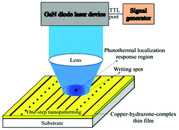
Semiconductor diode-based laser patterning with visible light has been extensively applied to the fabrication of arbitrary structures. However, recently, the technique has faced a great challenge because it cannot meet nanoscale-resolved patterning fabrication due to the optical diffraction limit, which is an inherent drawback in the field of optics. To attack the question, copper(II)–hydrazone-complex (CuL2) thin films are used as laser patterning materials. Under the heating of a writing laser spot, one-step laser nanopatterning on the CuL2 thin films is obtained. The convex-type and concave-type pattern structures are directly written without wet-etching and developing processes. The minimum pattern feature size is about 31 nm, which is far smaller than the diffraction limit and only ∼1/20 the writing spot size. Analysis indicates that the laser nanopatterning originates from obvious photothermal localization responses to the writing spot. Compared with common organic resists, the exposure dose of CuL2 is several orders higher than that of the polymer; thus CuL2 thin film materials are suitable for maskless direct laser writing lithography. This work also provides an effective method for one-step nanopatternings through diode-based laser writing at visible light wavelengths.
 Please wait while we load your content...

